High-Speed PCB Design Guide | Sierra Circuits
Download the High-Speed PCB Design Guide to design PCBs with signal frequencies from 50MHz to as high as 3GHz and beyond.| Sierra Circuits
Download the High-Speed PCB Design Guide to design PCBs with signal frequencies from 50MHz to as high as 3GHz and beyond.| Sierra Circuits
Download the Controlled Impedance Design Guide from Sierra Circuits. Explore the rest of our PCB design resources.| Sierra Circuits
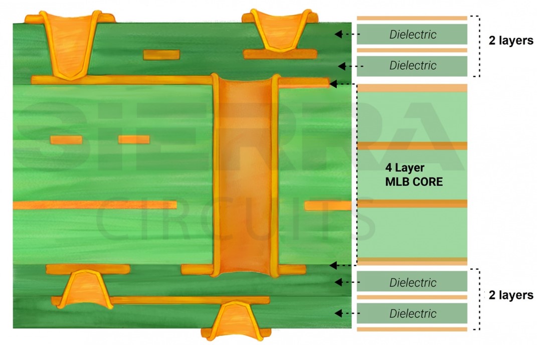
Vias are miniature conductive pathways drilled into the PCB to establish electrical connectivity between the different layers.| Sierra Circuits
Power integrity is one of the mind-boggling subjects when it comes to PCB designing. In this blog, we try to explain power integrity basics.| Sierra Circuits
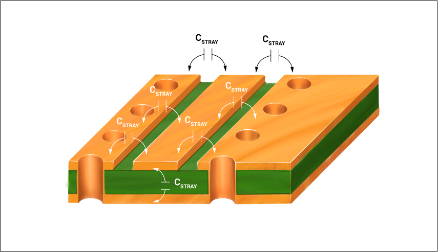
Parasitic capacitance effect in PCBs results in EMI and crosstalk. It can be reduced by following good layout practices.| Sierra Circuits
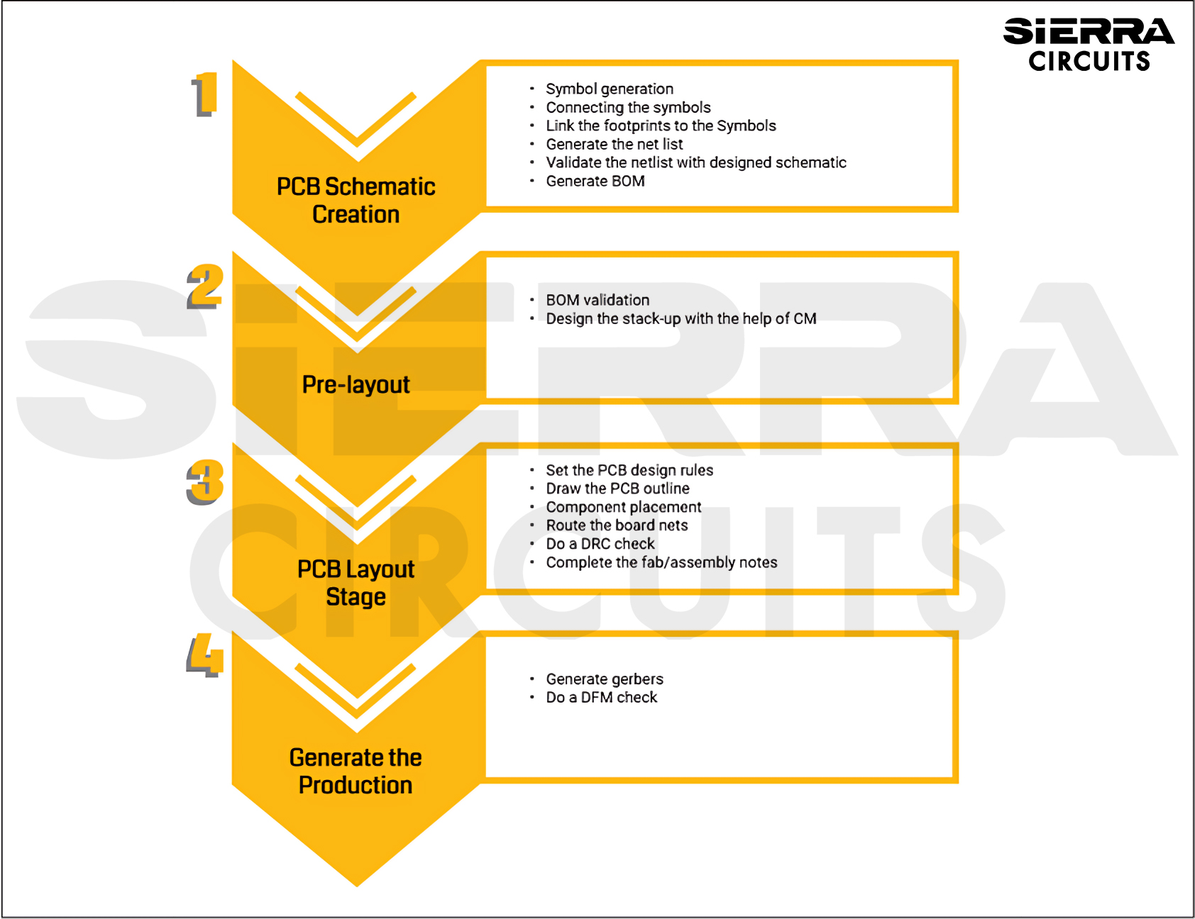
The PCB layout stage includes setting up the design tool, board outline, import of netlist, component placement, routing, silkscreen cleanup, and DRC check.| Sierra Circuits
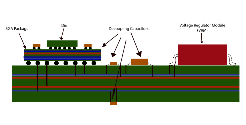
Understanding the operating range of frequencies is critical for decoupling capacitor placement to avoid EMI and EMC issues.| Sierra Circuits
In high-speed PCBs, the current return path follows the path of least impedance instead of least resistance. The current always comes back to the source.| Sierra Circuits
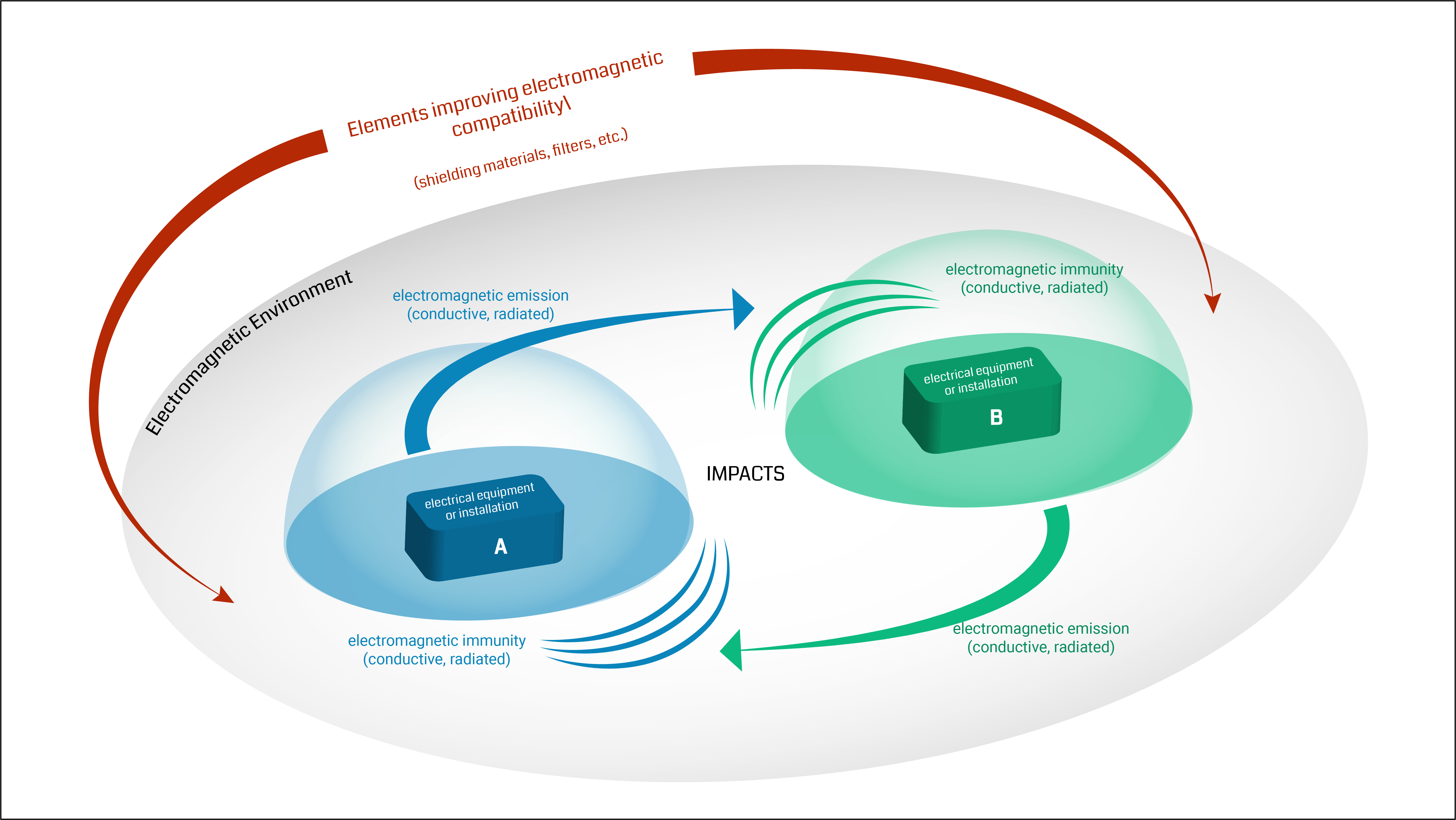
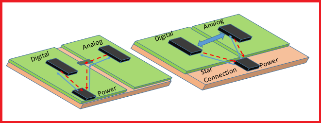
EMI can be mitigated by incorporating efficient grounding techniques and optimum trace spacing. This also ensures EMC.| Sierra Circuits
