How to Design a PCB Layout | Sierra Circuits
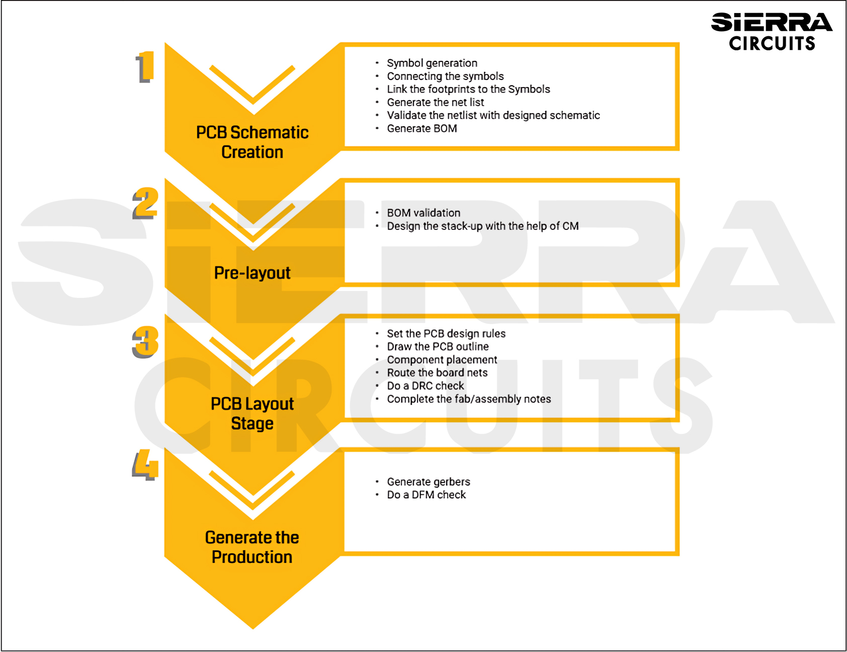
The PCB layout stage includes setting up the design tool, board outline, import of netlist, component placement, routing, silkscreen cleanup, and DRC check.| Sierra Circuits
The PCB layout stage includes setting up the design tool, board outline, import of netlist, component placement, routing, silkscreen cleanup, and DRC check.| Sierra Circuits
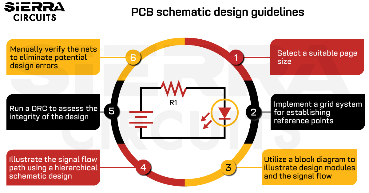
A PCB schematic must follow standard guidelines such as precision net labeling, and symbol standardization to have a well-structured design.| Sierra Circuits
