How to Design a PCB Layout | Sierra Circuits
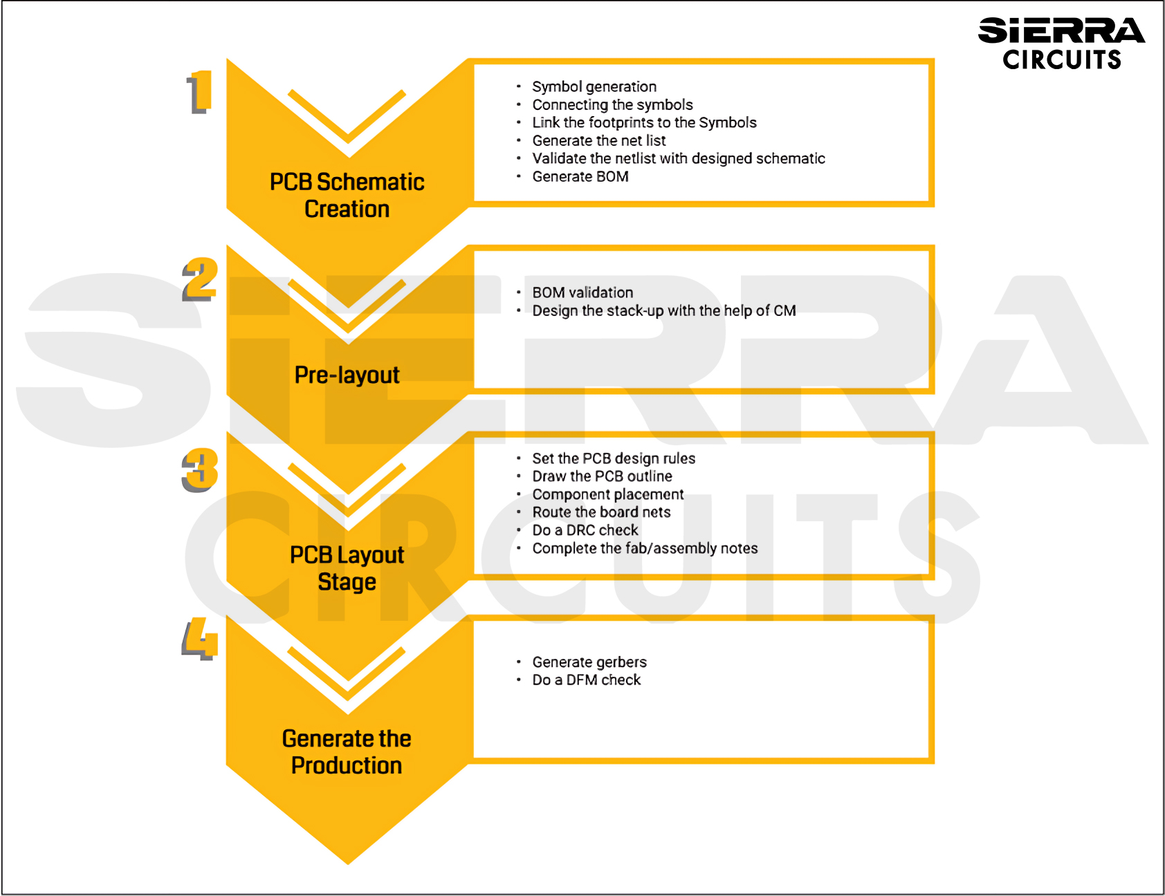
The PCB layout stage includes setting up the design tool, board outline, import of netlist, component placement, routing, silkscreen cleanup, and DRC check.| Sierra Circuits
A Cross Platform and Open Source Electronics Design Automation Suite| www.kicad.org
The PCB layout stage includes setting up the design tool, board outline, import of netlist, component placement, routing, silkscreen cleanup, and DRC check.| Sierra Circuits
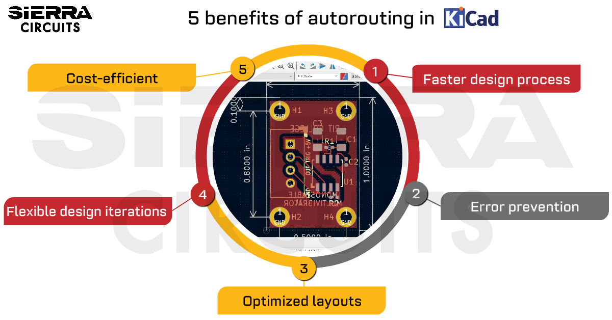
The autorouting plugin in KiCad automates the PCB routing process by creating optimized signal paths, improving the quality of your layouts.| Sierra Circuits
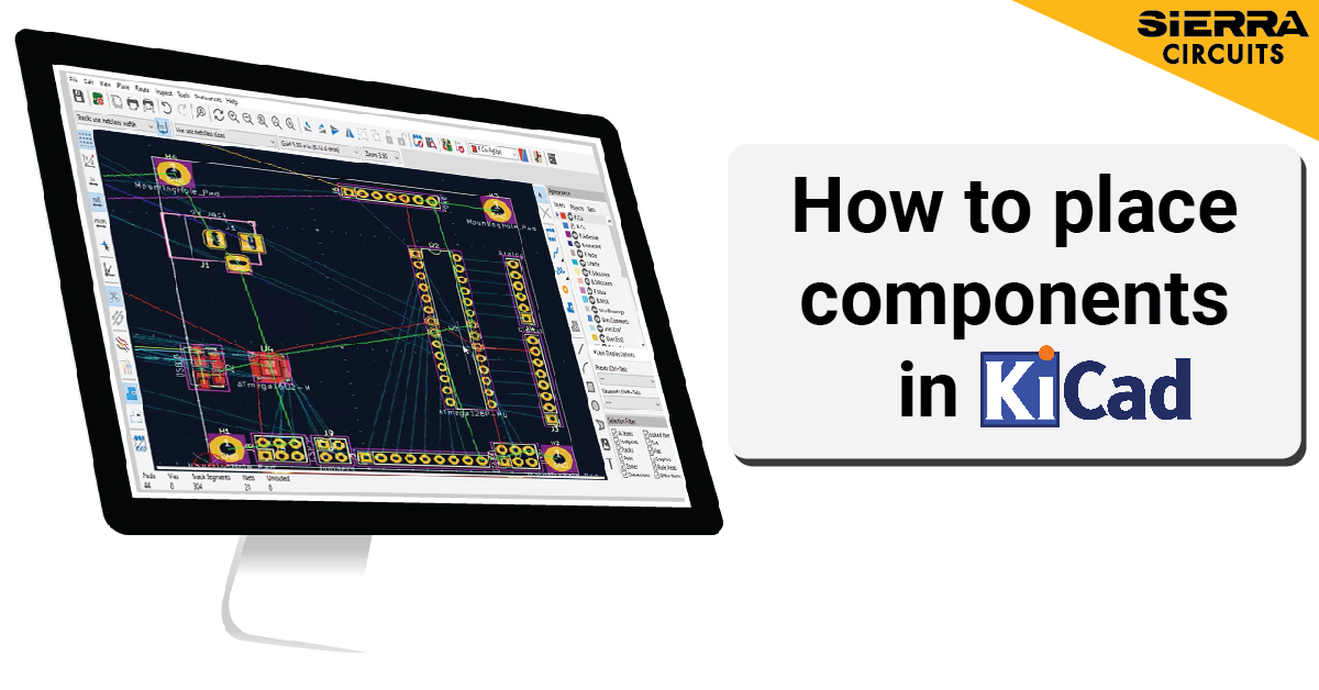
In this KiCad tutorial, you'll learn how to place components on your PCB layout and define your board outline.| Sierra Circuits
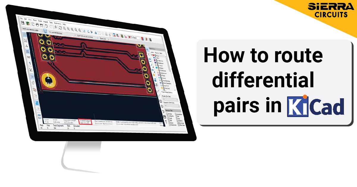
In this KiCad tutorial, you'll learn how to route differential pairs, fine-tune lengths, and manage skew to ensure signal integrity.| Sierra Circuits

In this KiCad tutorial, you will learn how to export IPC-2581, Gerber, and other production files such as drill files, netlist and BOM.| Sierra Circuits
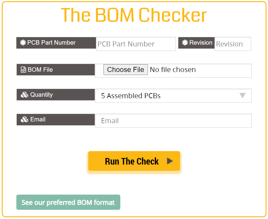
This BOM tool helps rectify the errors in the bill of materials list, get a cost estimation, and information regarding part availability.| Sierra Circuits

Download the KiCad Design Guide from Sierra Circuits. Learn how to PCB design using KiCad and explore the rest of our PCB Design resources.| Sierra Circuits
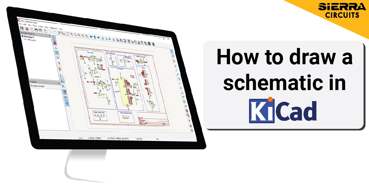
In this KiCad tutorial, you will learn how to create a schematic and build a custom symbol library from scratch.| Sierra Circuits
