Connector Design Guide | Sierra Circuits
Download the Connector Design Guide which helps you select the right connector and covers terminology, selection and layout rules, and more.| Sierra Circuits
Download the Connector Design Guide which helps you select the right connector and covers terminology, selection and layout rules, and more.| Sierra Circuits
In this tutorial, you'll learn how to set up design rules in KiCad, such as trace width, clearance, via size, and net classes.| Sierra Circuits

PCB fabrication considerations for proper component placement are essential to improve the signal quality and performance of your device.| Sierra Circuits
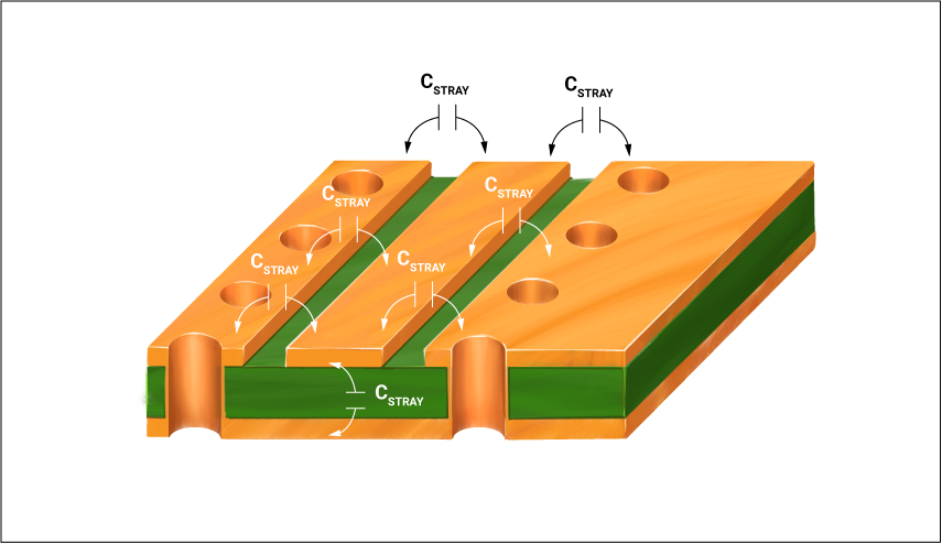
Parasitic capacitance effect in PCBs results in EMI and crosstalk. It can be reduced by following good layout practices.| Sierra Circuits
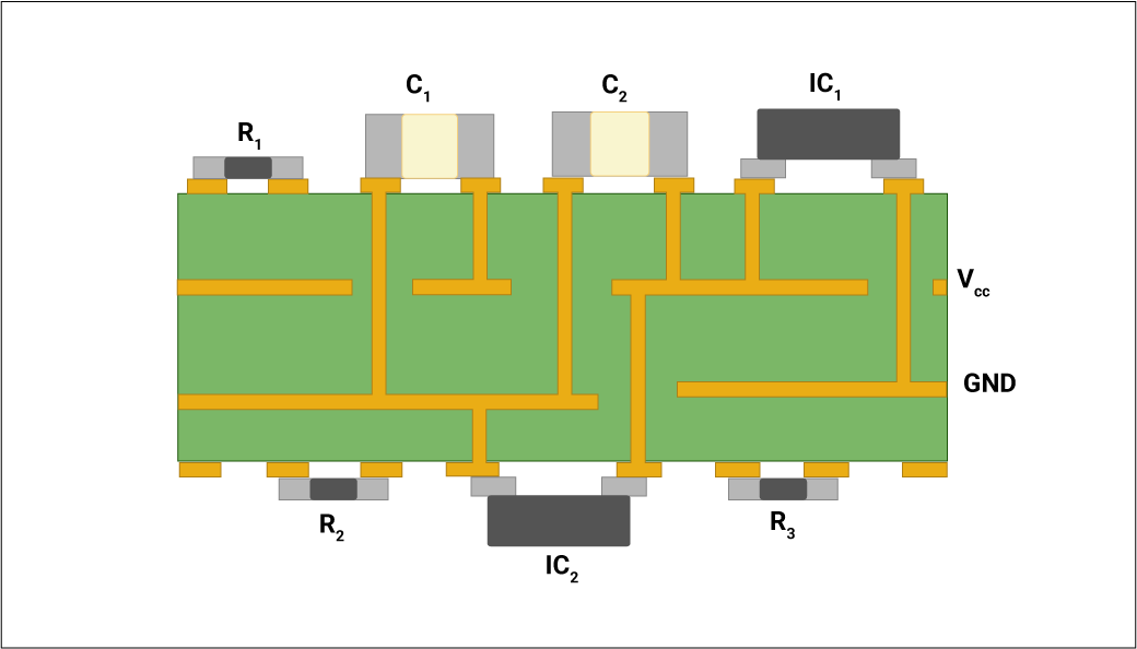
Understanding the operating range of frequencies is critical for decoupling capacitor placement to avoid EMI and EMC issues.| Sierra Circuits
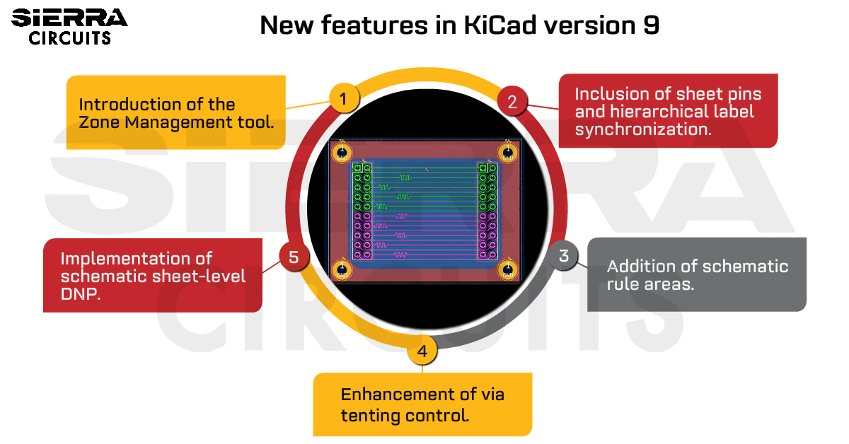
KiCad version 9 is set to add features like the new zone manager, sheet pin and label synchronization, and schematic sheet-level DNP.| Sierra Circuits
Download the KiCad Design Guide from Sierra Circuits. Learn how to PCB design using KiCad and explore the rest of our PCB Design resources.| Sierra Circuits
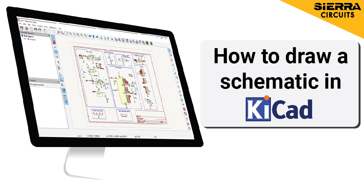
In this KiCad tutorial, you will learn how to create a schematic and build a custom symbol library from scratch.| Sierra Circuits
