How to Set Up Design Rules in KiCad | Sierra Circuits
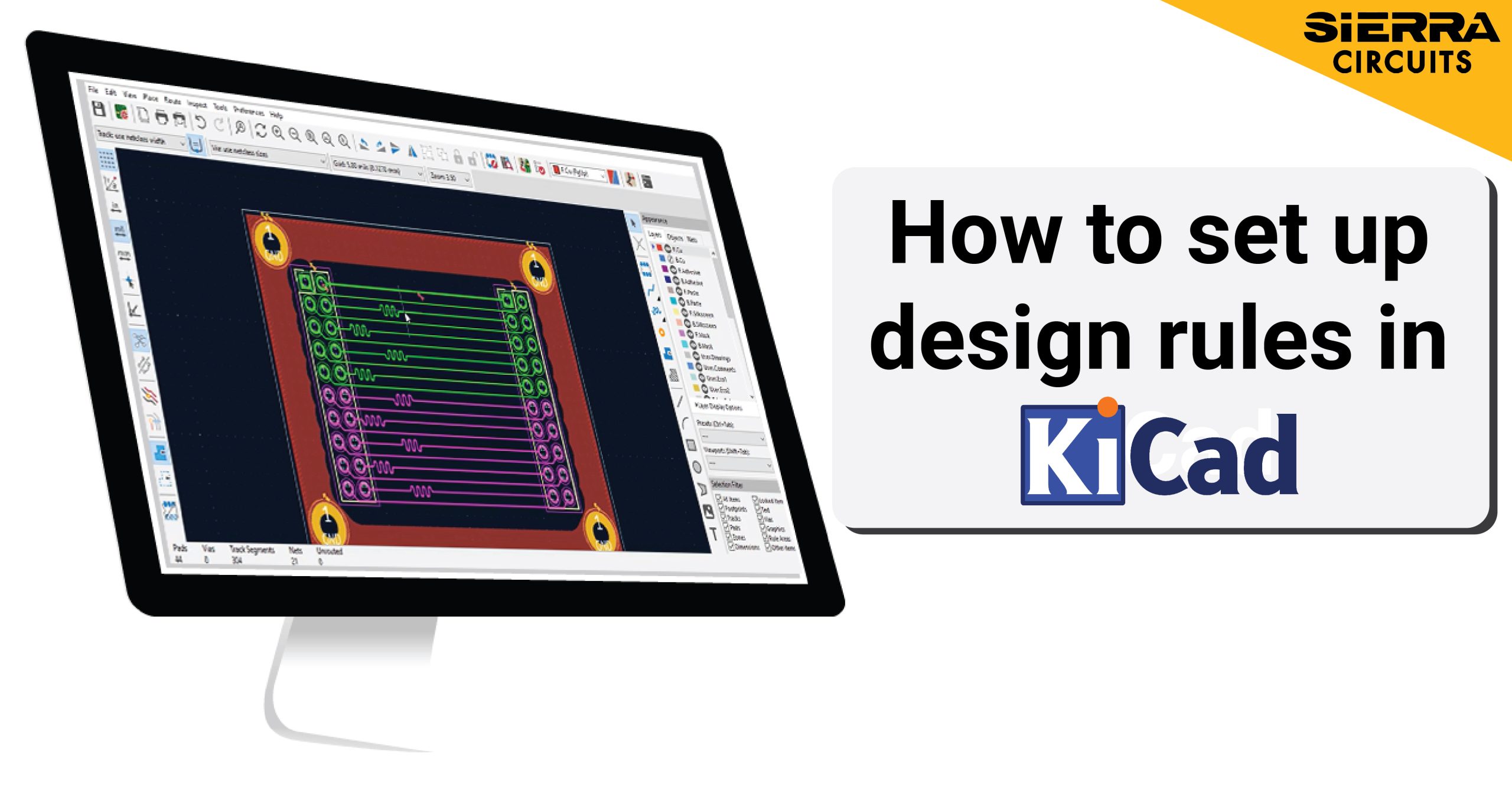
In this tutorial, you'll learn how to set up design rules in KiCad, such as trace width, clearance, via size, and net classes.| Sierra Circuits
In this tutorial, you'll learn how to set up design rules in KiCad, such as trace width, clearance, via size, and net classes.| Sierra Circuits

PCB fabrication considerations for proper component placement are essential to improve the signal quality and performance of your device.| Sierra Circuits
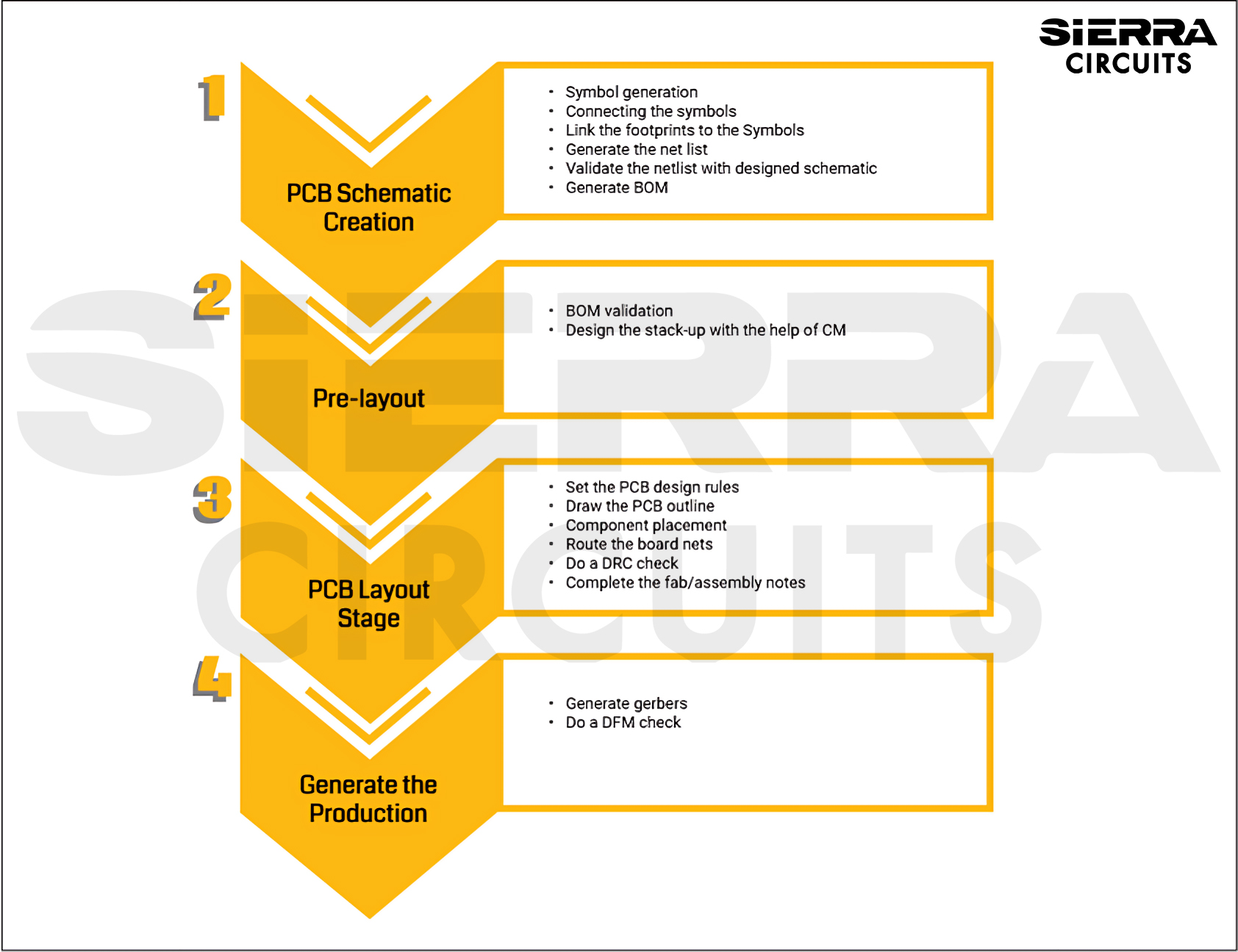
The PCB layout stage includes setting up the design tool, board outline, import of netlist, component placement, routing, silkscreen cleanup, and DRC check.| Sierra Circuits
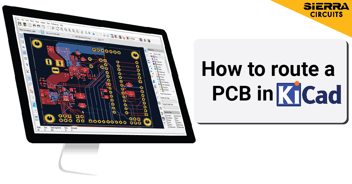
PCB routing in KiCad includes adding ground pours, managing power routing, handling differential pairs, and orthogonal routing.| Sierra Circuits

Download the KiCad Design Guide from Sierra Circuits. Learn how to PCB design using KiCad and explore the rest of our PCB Design resources.| Sierra Circuits
Sierra Circuits Canada was established in 2022 to service the PCB manufacturing and assembly needs of our Canadian and worldwide customers.| Sierra Circuits
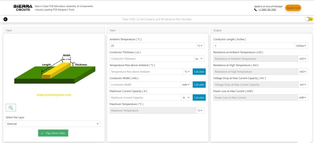
The Trace Width, Current, and Temperature Rise Calculator helps you compute conductor width, current capacity, and temperature above ambient.| Sierra Circuits
