How to Build a Multilayer PCB Stack-up | Sierra Circuits
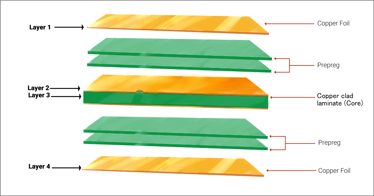
A multilayer PCB has more than two layers in its stack-up. The stack-up describes the construction of a multilayer board in sequential order.| Sierra Circuits
A multilayer PCB has more than two layers in its stack-up. The stack-up describes the construction of a multilayer board in sequential order.| Sierra Circuits

To build an efficient PCB stack-up, select the right materials, estimate the number of signal layers, and optimally arrange the layers.| Sierra Circuits
Download the High-Speed PCB Design Guide to design PCBs with signal frequencies from 50MHz to as high as 3GHz and beyond.| Sierra Circuits
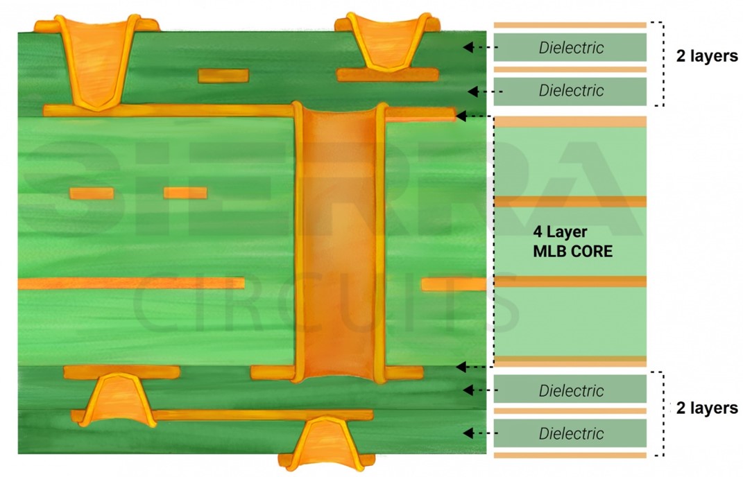
Vias are miniature conductive pathways drilled into the PCB to establish electrical connectivity between the different layers.| Sierra Circuits
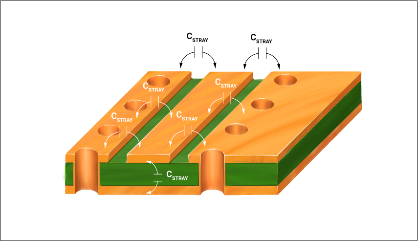
Parasitic capacitance effect in PCBs results in EMI and crosstalk. It can be reduced by following good layout practices.| Sierra Circuits
In high-speed PCBs, the current return path follows the path of least impedance instead of least resistance. The current always comes back to the source.| Sierra Circuits
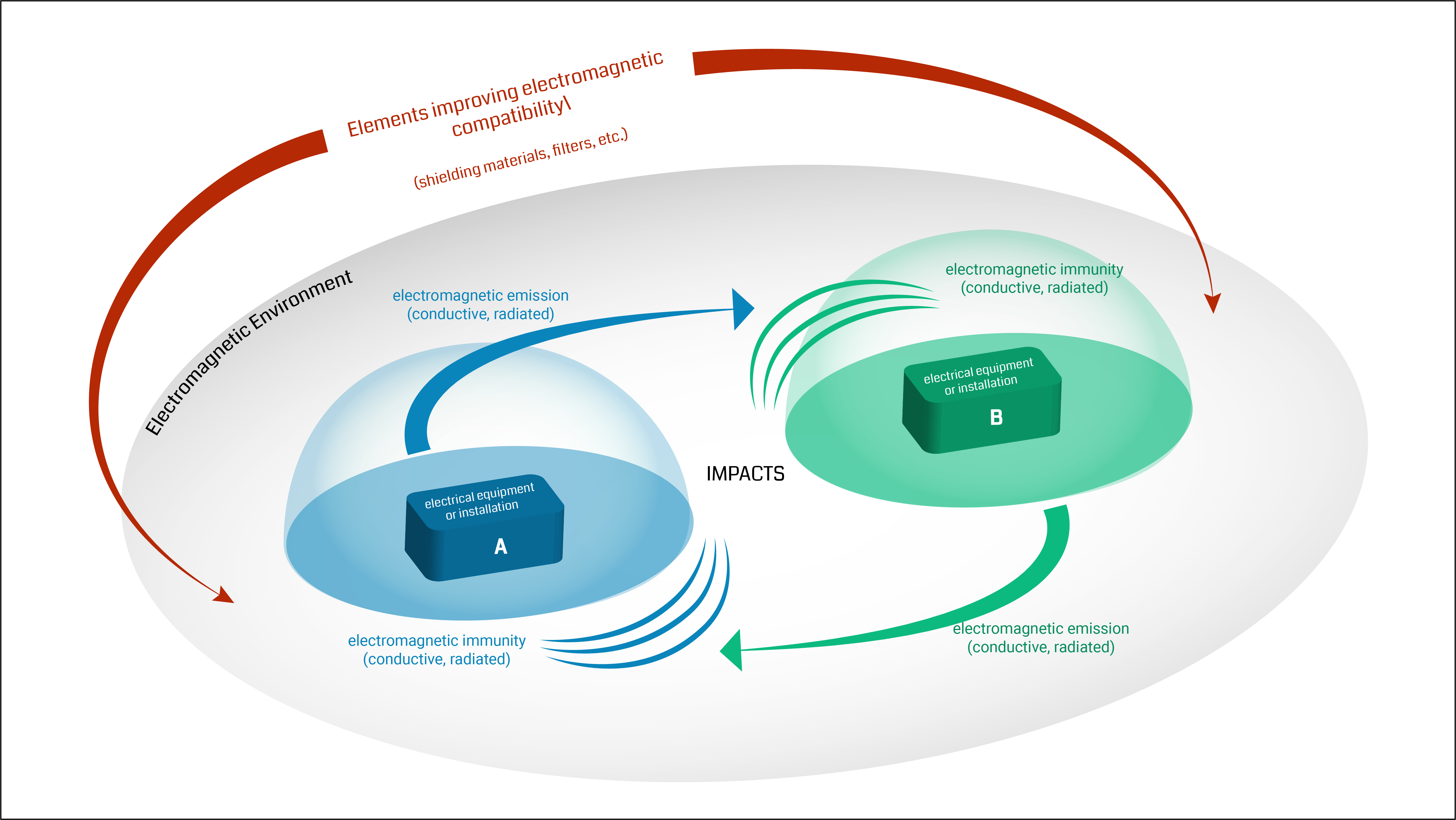
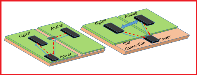
EMI can be mitigated by incorporating efficient grounding techniques and optimum trace spacing. This also ensures EMC.| Sierra Circuits
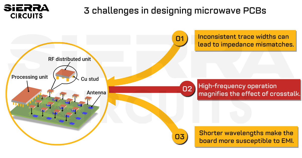
To design a microwave PCB, select materials with low dielectric constant, prefer CPWs, and add board-level shielding to mitigate EMI effects.| Sierra Circuits
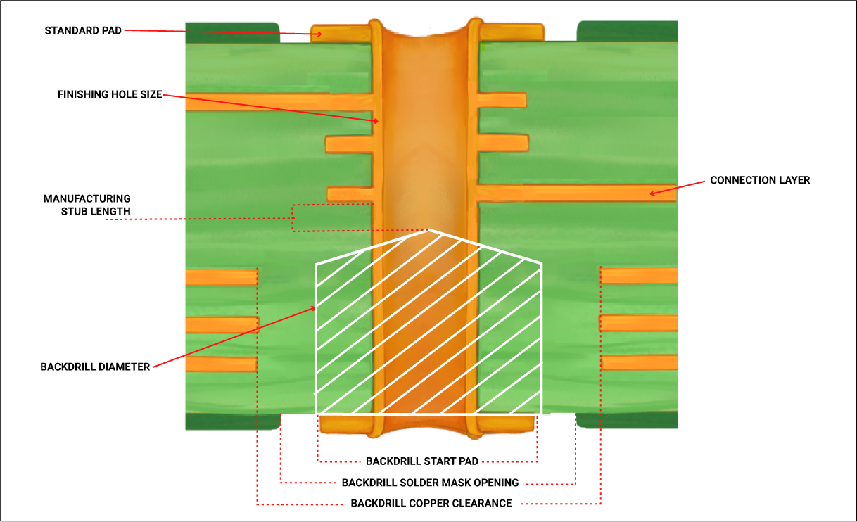
Back drilling in PCB involves drilling a hole slightly larger in diameter than the PTH to remove the conductive via stub.| Sierra Circuits
