
PCB Design for Assembly Handbook Download | Sierra Circuits
Download the Design for Assembly Handbook from Sierra Circuits and explore the rest of our PCB design resources.| Sierra Circuits
Download the Design for Assembly Handbook from Sierra Circuits and explore the rest of our PCB design resources.| Sierra Circuits
PCB assembly process involves DFA, SMT and through-hole components placement, testing, and final inspection.| Sierra Circuits
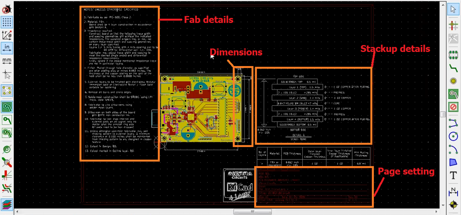
A PCB fab drawing is a reference document for manufacturing and includes all the information like board outline, stack-up, drilled holes, etc.| Sierra Circuits
Computer-Aided Manufacturing for PCBs is the use of software and computer-controlled machinery to perform tasks like drilling and component insertion.| Sierra Circuits
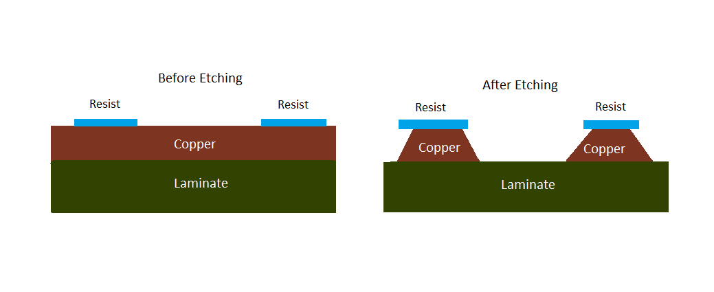
Wet PCB etching is a process of removing unwanted copper by immersing a circuit board in a chemical solution (acidic or alkaline based).| Sierra Circuits
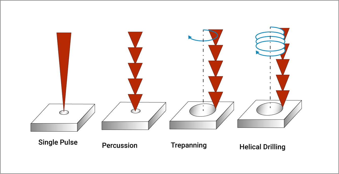
Laser drilling is performed to drill holes and vias on a PCB using a laser beam without compromising the board integrity.| Sierra Circuits
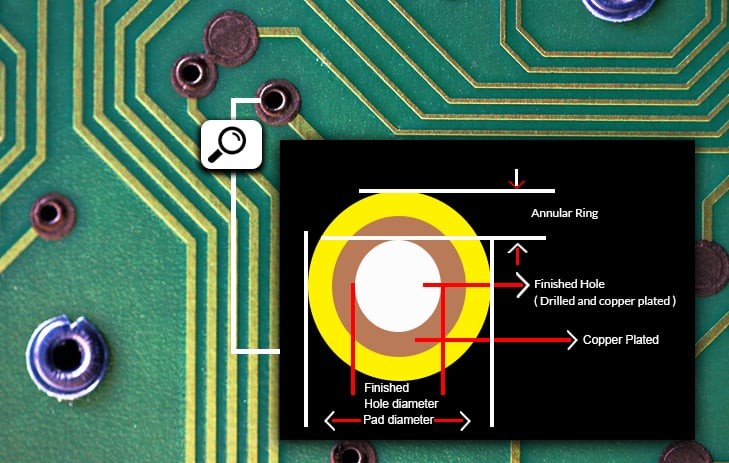
An annular ring is the copper area surrounding a plated via on a PCB. It establishes a solid connection between the via and copper traces.| Sierra Circuits
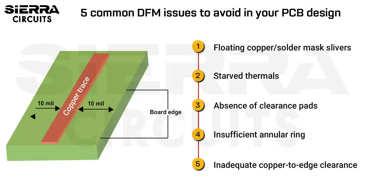
DFM checks each design before going for fabrication. It predicts potential defects and ensures board manufacturing with exact specifications.| Sierra Circuits
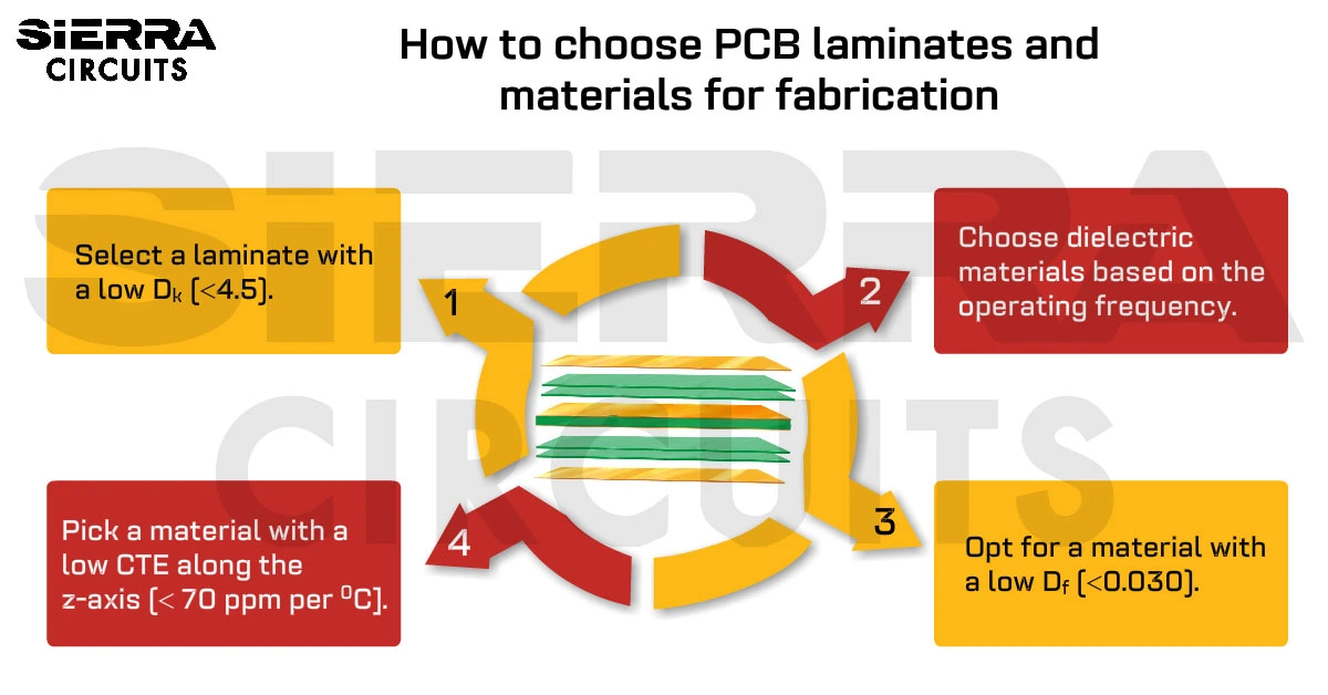
Selecting the right PCB laminates and materials for your design is very important as it can impact the overall performance of the board.| Sierra Circuits

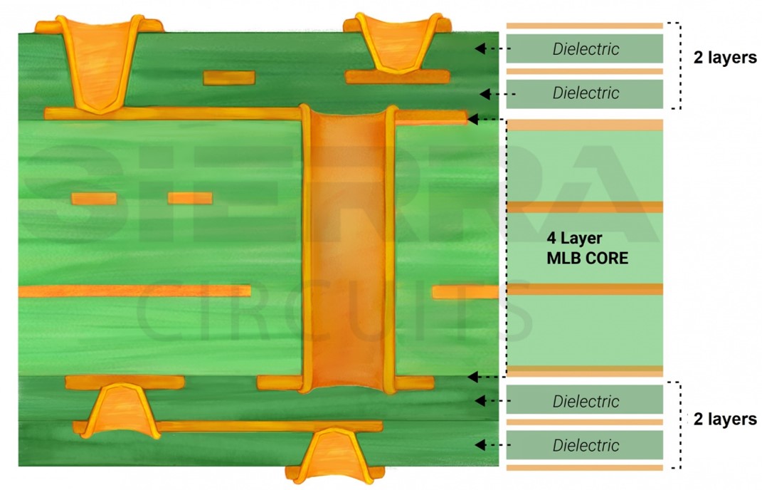
To build an efficient PCB stack-up, select the right materials, estimate the number of signal layers, and optimally arrange the layers.| Sierra Circuits
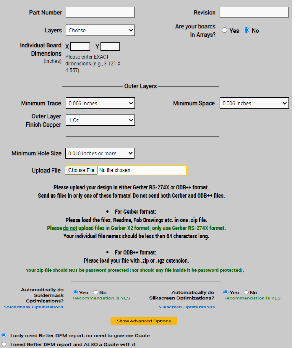
Better DFM is an online design tool that checks for the manufacturability of an electronic circuit design. Try it now!| Sierra Circuits
Vias are miniature conductive pathways drilled into the PCB to establish electrical connectivity between the different layers.| Sierra Circuits

Sierra Circuits builds your quickturn high-quality rigid PCB prototype. Contact our engineering team to learn about our PCB fab capabilities.| Sierra Circuits
