PCB Material Selector | Sierra Circuits
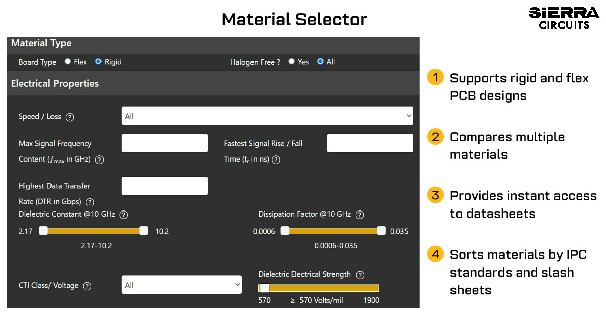
Use this PCB material selector before you send your design to manufacturing and find materials that suit your application. Try it now!| Sierra Circuits
Use this PCB material selector before you send your design to manufacturing and find materials that suit your application. Try it now!| Sierra Circuits
Sierra Circuits offers one-stop PCB assembly services in our Silicon Valley location. Get a quote today for your PCBA needs.| Sierra Circuits
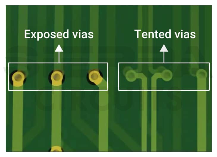
PCB via tenting protects vias from contamination, corrosion, and electrical shorts by covering exposed vias with a solder mask.| Sierra Circuits
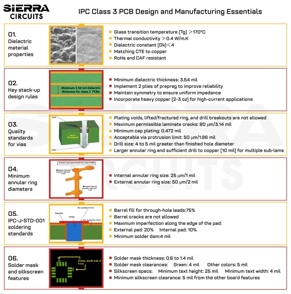
To build an efficient class 3 PCB, you need to design your stack-up, annular ring, and vias as per the IPC-6012 and IPC-A-610 standards.| Sierra Circuits

Originally published at: https://www.protoexpress.com/blog/how-to-design-reliable-microvias-in-your-pcbs/ Microvia failure occurs due to the thermal stresses that arise during the PCB assembly process. These stresses can have a significant impact on the reliability of the plated hole. Key design strategies for enhancing microvia reliability include selecting suitable materials for laser drilling, adhering to IPC-T-50M guidelines, and implementing stack-up configurations in alignment with IPC...| SierraConnect
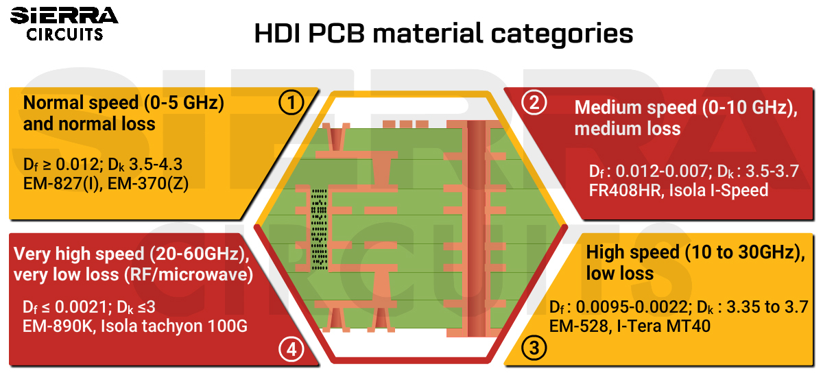
When choosing HDI PCB material, consider the operating frequency, acceptable signal loss, and laser drilling compatibility.| Sierra Circuits

Download the Design for Manufacturing Handbook and learn the best design practices for your electronics in terms of both cost and complexity.| Sierra Circuits
Sierra Circuits offers quickturn, high-quality, HDI printed circuit boards. Learn about our HDI PCB capabilities.| Sierra Circuits

To build an efficient PCB stack-up, select the right materials, estimate the number of signal layers, and optimally arrange the layers.| Sierra Circuits
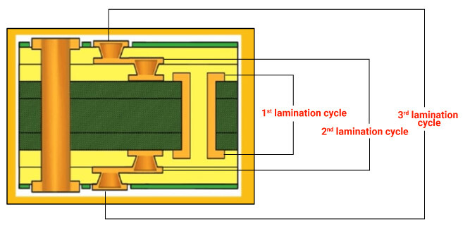
Sequential lamination is a process of fabricating a high-density PCB using cores and subsets composed of copper and dielectric layers.| Sierra Circuits
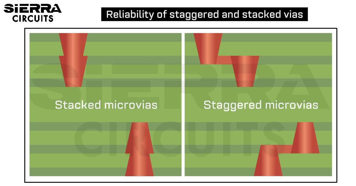
Staggered and stacked vias play crucial role in designing HDI boards. The compact design is highly functional with great signal integrity.| Sierra Circuits
