

Download the HDI PCB Design Guide which provides tons of guidelines for blind and buried via technology.| Sierra Circuits

To build an efficient PCB stack-up, select the right materials, estimate the number of signal layers, and optimally arrange the layers.| Sierra Circuits
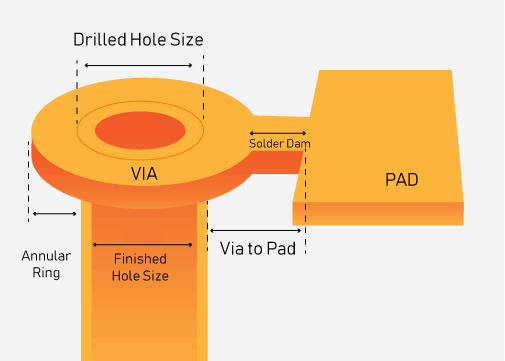
Drilling is the most expensive and time-consuming process in PCB manufacturing. A small fault in the drilling process leads to a great loss.| Sierra Circuits

PCB fabrication considerations for proper component placement are essential to improve the signal quality and performance of your device.| Sierra Circuits
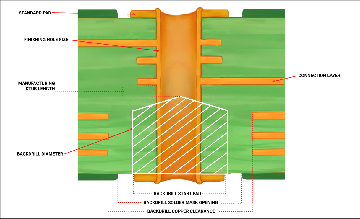
Back drilling in PCB involves drilling a hole slightly larger in diameter than the PTH to remove the conductive via stub.| Sierra Circuits