
Online PCB Manufacturing and Assembly Quotes | Sierra Circuits
Welcome to Sierra Circuits, your go-to solution for top-tier electronics, offering online PCB manufacturing and assembly quotes.| Sierra Circuits
Welcome to Sierra Circuits, your go-to solution for top-tier electronics, offering online PCB manufacturing and assembly quotes.| Sierra Circuits
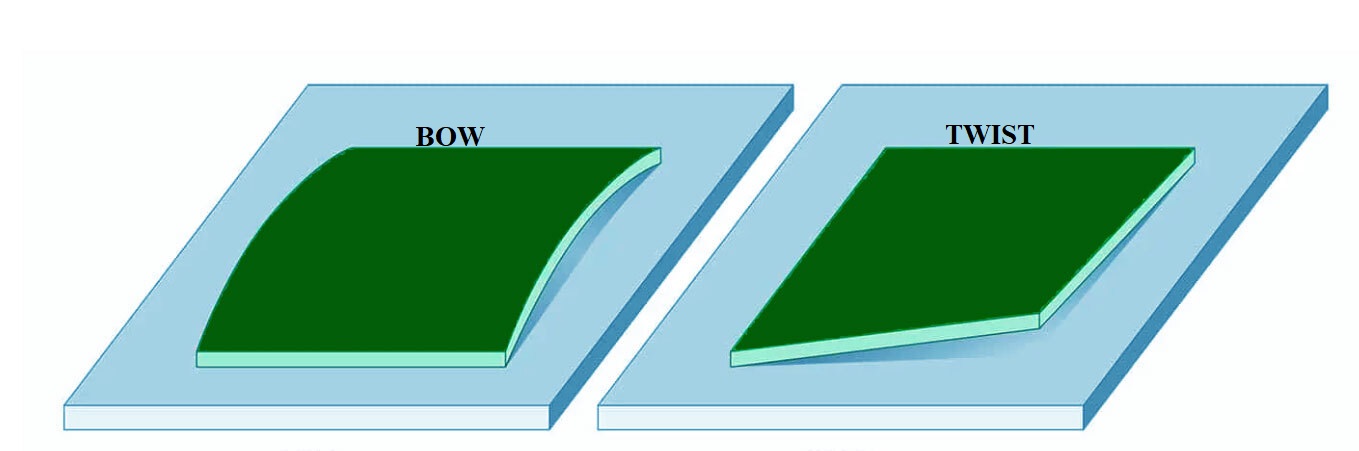
The PCB Stack-Up Design Guide helps you build efficient stack-ups with improved SI, power distribution, and heat dissipation. Download now!| Sierra Circuits
PCB layer count estimation is a critical step to achieving design success as it directly impacts the functional capability of your board.| Sierra Circuits
Balanced copper distribution in your PCB design can be achieved by incorporating copper thieving and hatch patterns.| Sierra Circuits
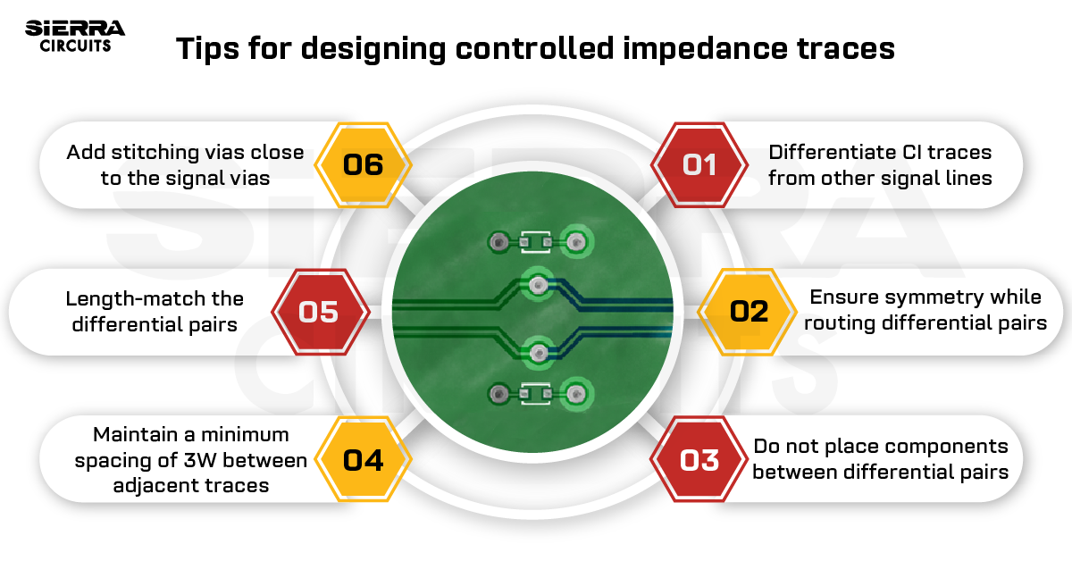
PCB materials, dielectric constant, trace height, and width affect the controlled impedance of a transmission line.| Sierra Circuits
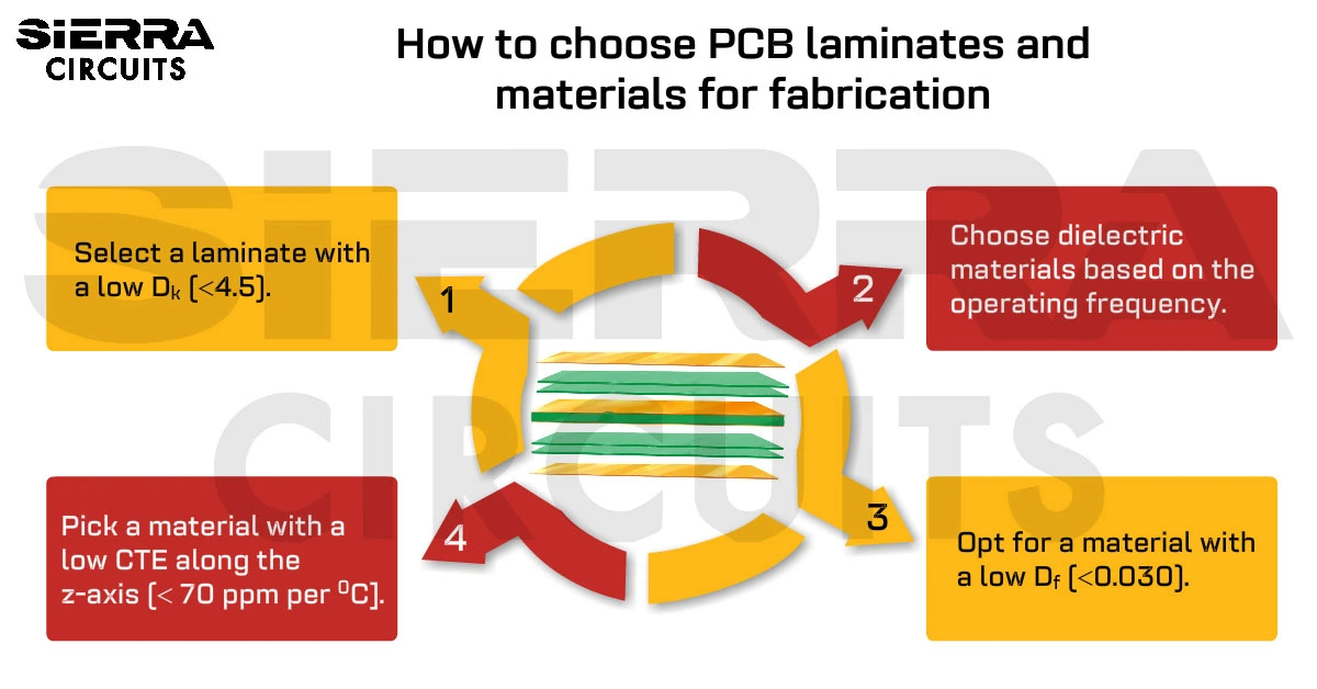
Selecting the right PCB laminates and materials for your design is very important as it can impact the overall performance of the board.| Sierra Circuits
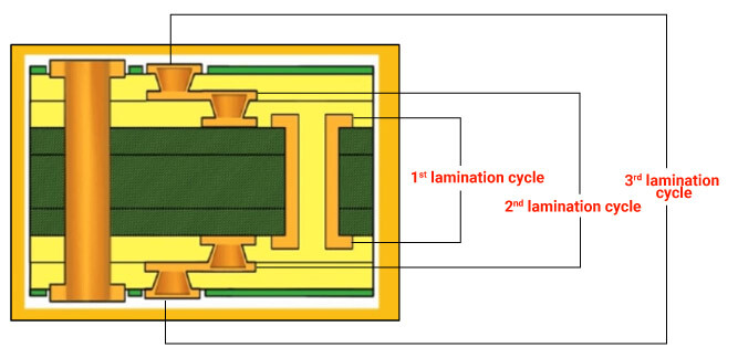
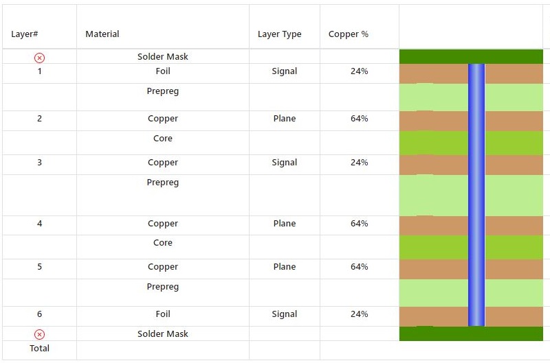
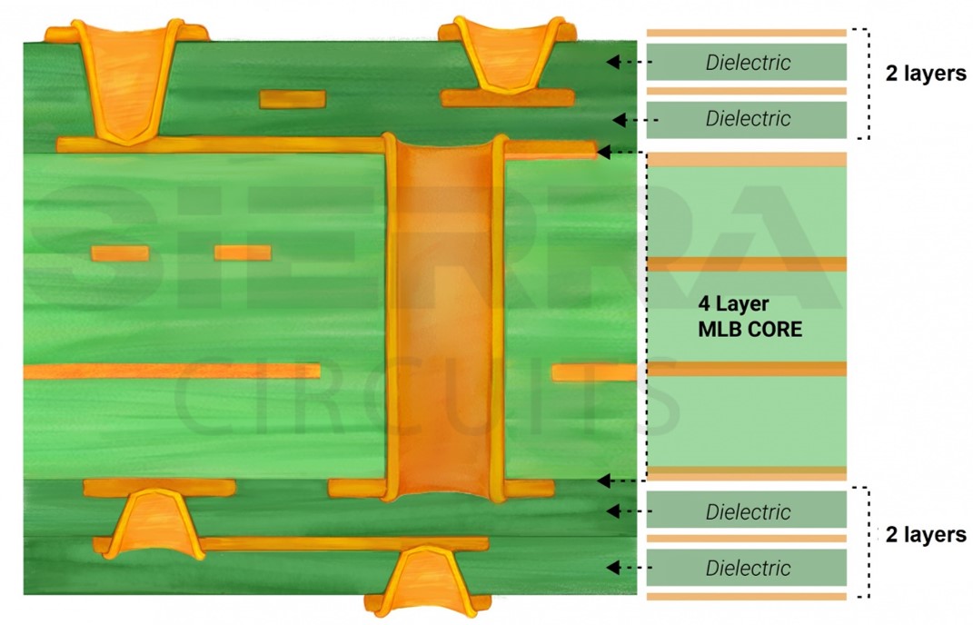
Sequential lamination is a process of fabricating a high-density PCB using cores and subsets composed of copper and dielectric layers.| Sierra Circuits
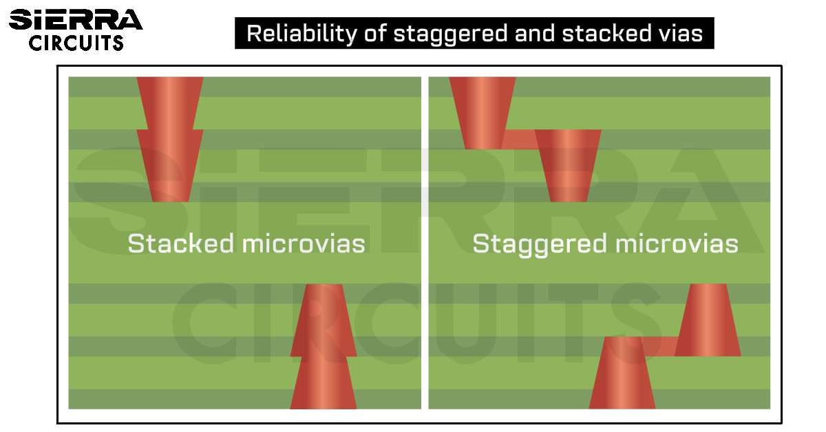
Staggered and stacked vias play crucial role in designing HDI boards. The compact design is highly functional with great signal integrity.| Sierra Circuits
Drilling is the most expensive and time-consuming process in PCB manufacturing. A small fault in the drilling process leads to a great loss.| Sierra Circuits
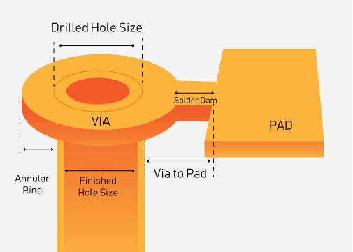
Vias are miniature conductive pathways drilled into the PCB to establish electrical connectivity between the different layers.| Sierra Circuits
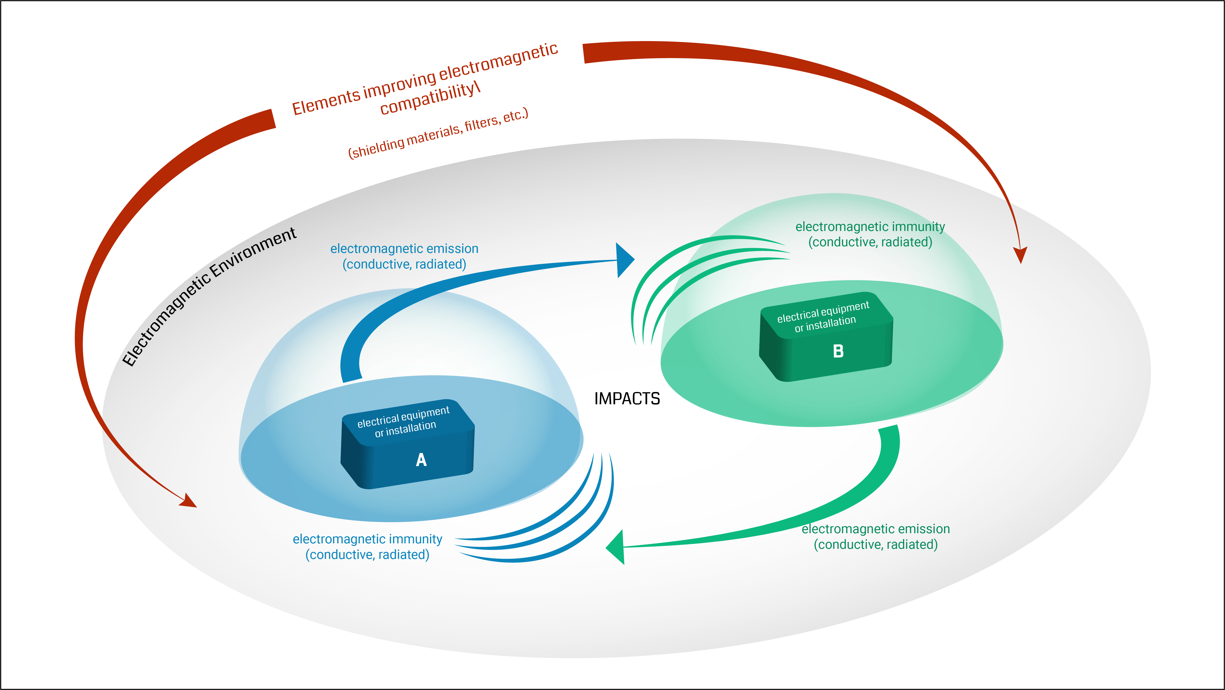
EMI can be mitigated by incorporating efficient grounding techniques and optimum trace spacing. This also ensures EMC.| Sierra Circuits
