
PCB Design for Assembly Handbook Download | Sierra Circuits
Download the Design for Assembly Handbook from Sierra Circuits and explore the rest of our PCB design resources.| Sierra Circuits
Download the Design for Assembly Handbook from Sierra Circuits and explore the rest of our PCB design resources.| Sierra Circuits

Download the Design for Manufacturing Handbook and learn the best design practices for your electronics in terms of both cost and complexity.| Sierra Circuits
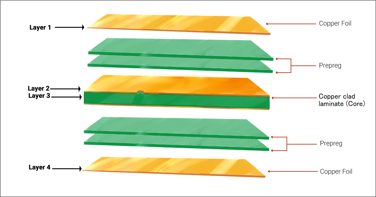
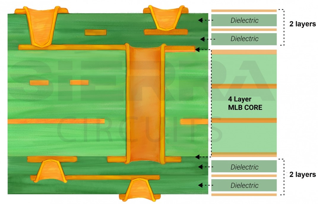
A multilayer PCB has more than two layers in its stack-up. The stack-up describes the construction of a multilayer board in sequential order.| Sierra Circuits
In this tutorial, you'll learn how to set up design rules in KiCad, such as trace width, clearance, via size, and net classes.| Sierra Circuits
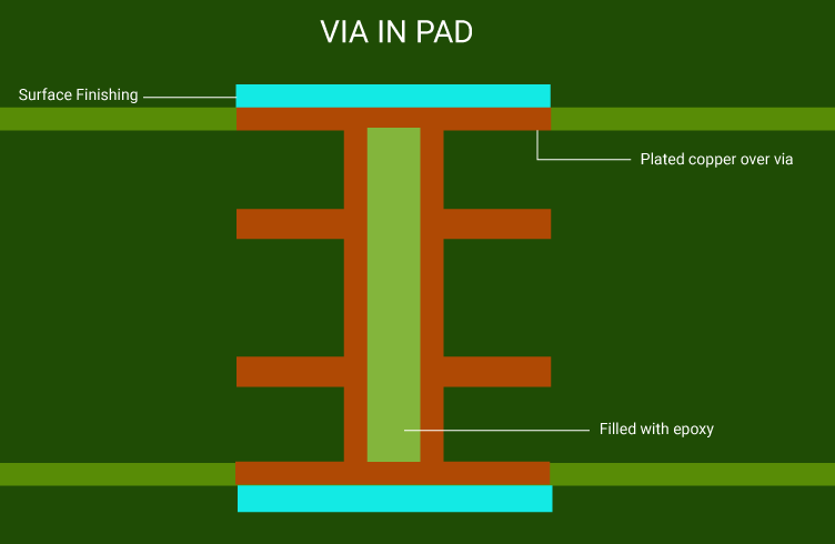
Use via-in-pad technology when the board size is limited, components have small footprints, and surface routing options are restricted.| Sierra Circuits
Drilling is the most expensive and time-consuming process in PCB manufacturing. A small fault in the drilling process leads to a great loss.| Sierra Circuits
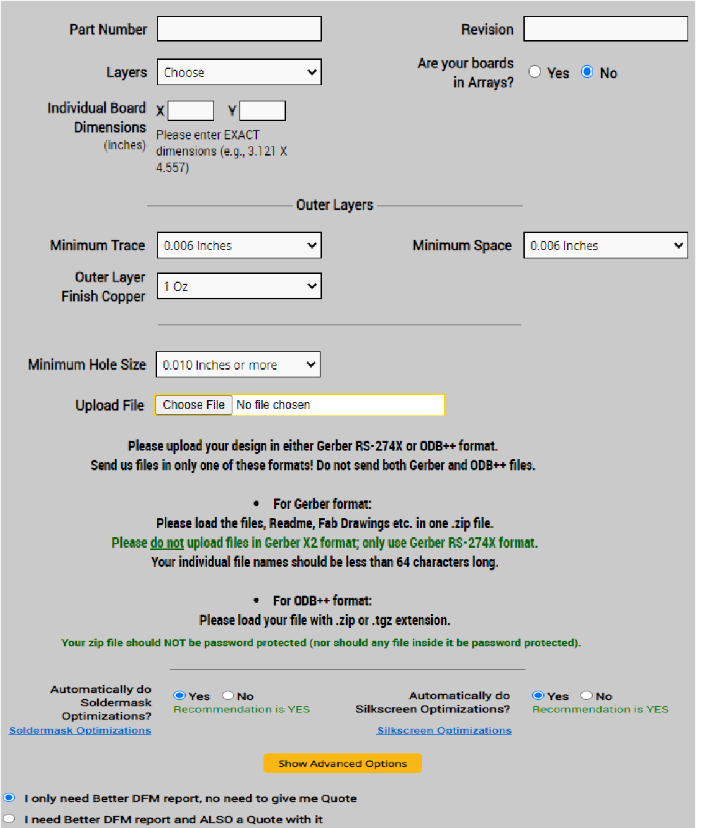
Better DFM is an online design tool that checks for the manufacturability of an electronic circuit design. Try it now!| Sierra Circuits
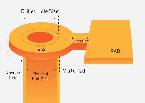
Vias are miniature conductive pathways drilled into the PCB to establish electrical connectivity between the different layers.| Sierra Circuits
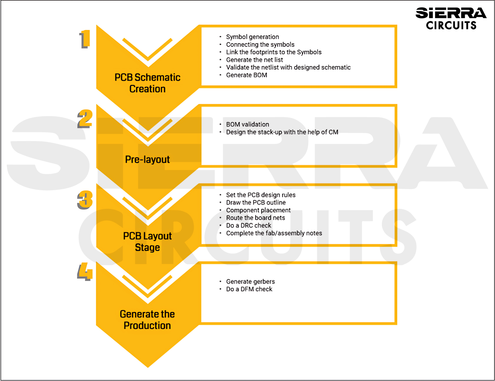
The PCB layout stage includes setting up the design tool, board outline, import of netlist, component placement, routing, silkscreen cleanup, and DRC check.| Sierra Circuits
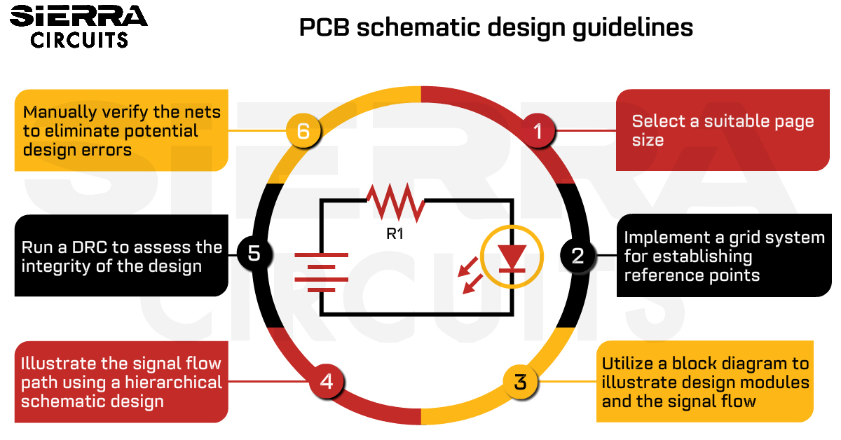
A PCB schematic must follow standard guidelines such as precision net labeling, and symbol standardization to have a well-structured design.| Sierra Circuits
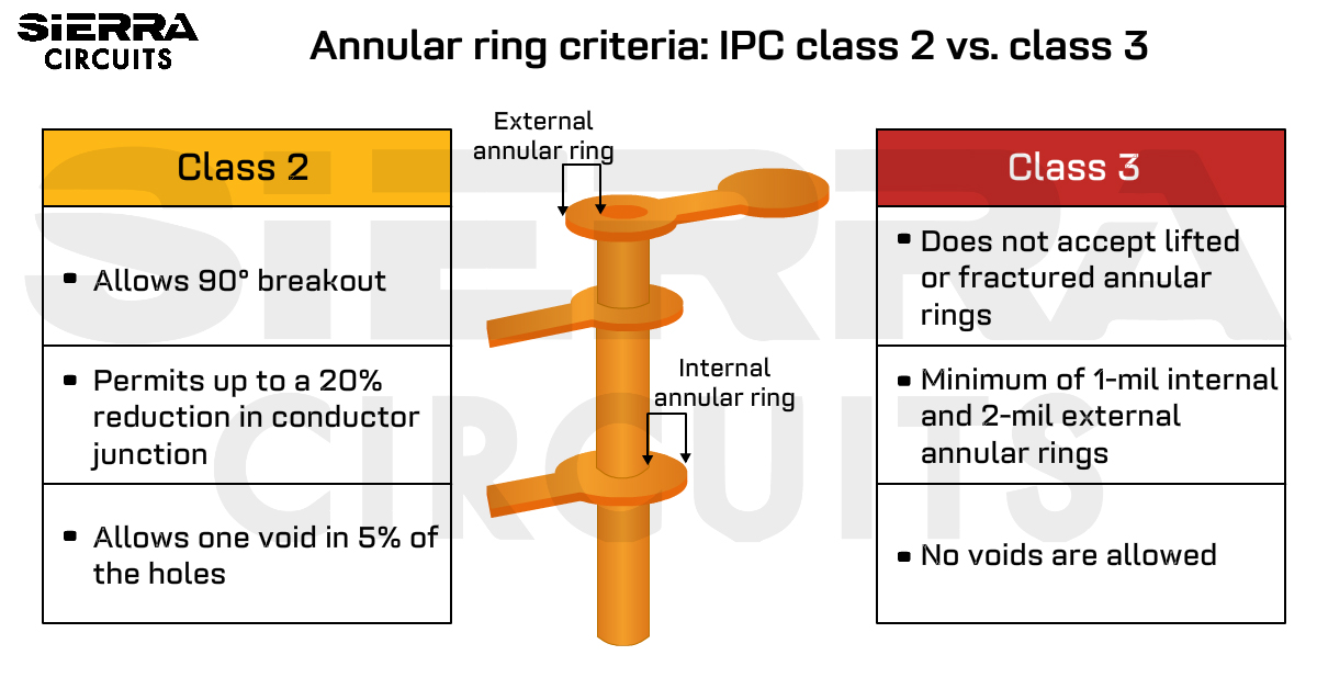
This article will help you understand the different PCB design rules for IPC Class 2 and Class 3 printed circuit boards.| Sierra Circuits
