What Should a PCB Fab Drawing Include? | Sierra Circuits
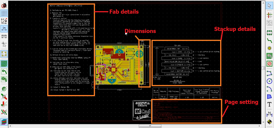
A PCB fab drawing is a reference document for manufacturing and includes all the information like board outline, stack-up, drilled holes, etc.| Sierra Circuits
A PCB fab drawing is a reference document for manufacturing and includes all the information like board outline, stack-up, drilled holes, etc.| Sierra Circuits
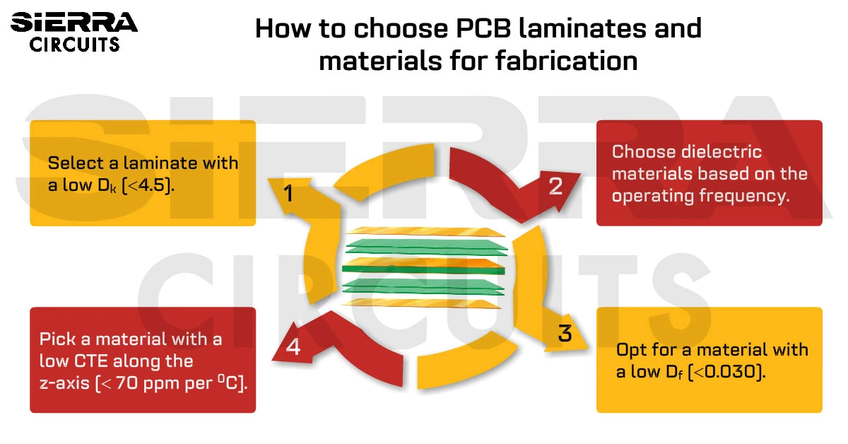
Selecting the right PCB laminates and materials for your design is very important as it can impact the overall performance of the board.| Sierra Circuits

Download the Design for Manufacturing Handbook and learn the best design practices for your electronics in terms of both cost and complexity.| Sierra Circuits

To build an efficient PCB stack-up, select the right materials, estimate the number of signal layers, and optimally arrange the layers.| Sierra Circuits
Here are some best high-speed PCB routing practices that will help PCB designers to craft a perfect design.| Sierra Circuits
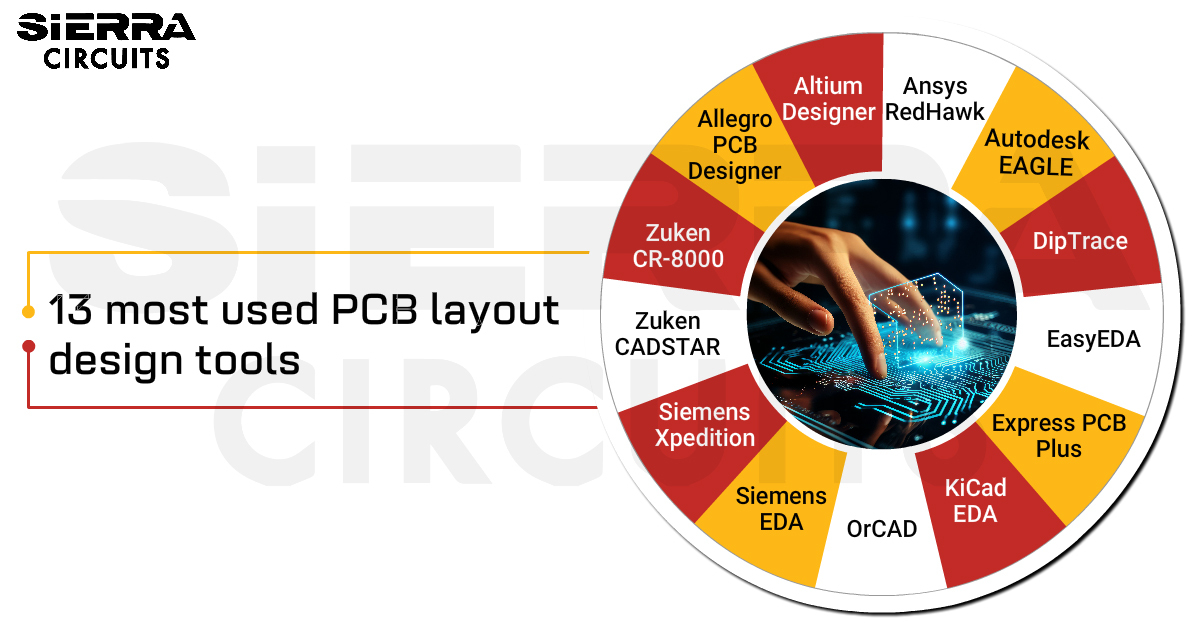
Some of the most used PCB layout design tools are Altium, Allegro, and KiCad. Consider UI, routing, and simulation before selecting one.| Sierra Circuits
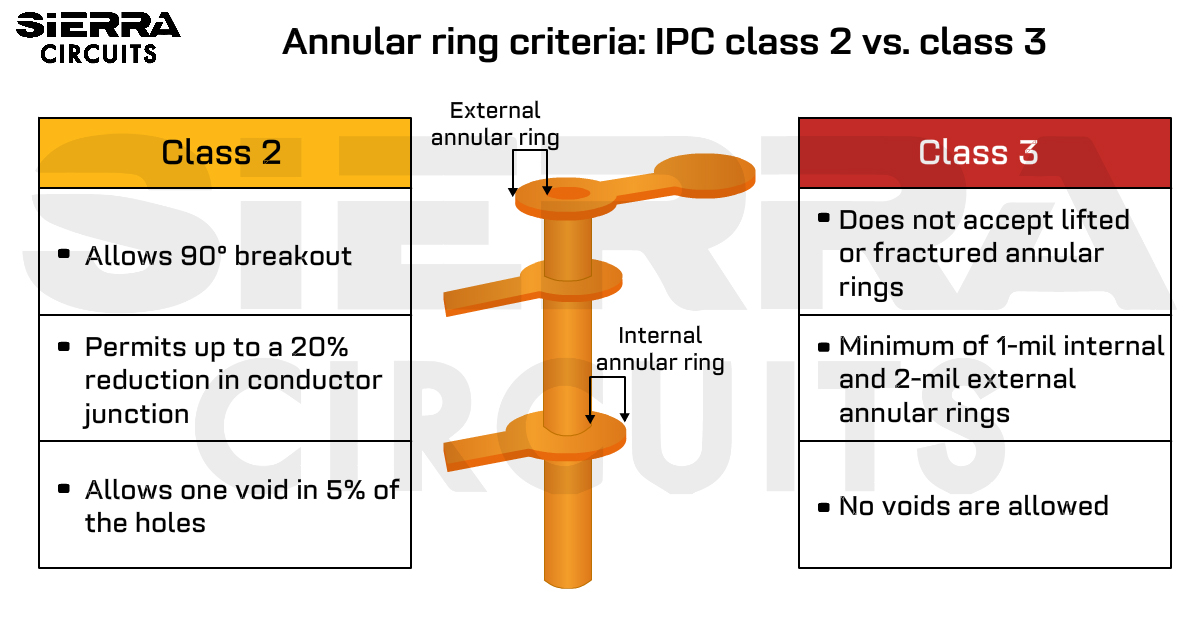
This article will help you understand the different PCB design rules for IPC Class 2 and Class 3 printed circuit boards.| Sierra Circuits
