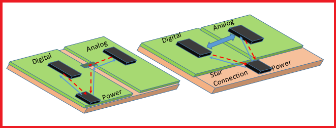
9 Factors that Cause Signal Integrity Issues | Sierra Circuits
Avoiding signal integrity issues in a PCB is a complex task for designers. It requires a deep understanding of design rules and techniques.| Sierra Circuits
Avoiding signal integrity issues in a PCB is a complex task for designers. It requires a deep understanding of design rules and techniques.| Sierra Circuits
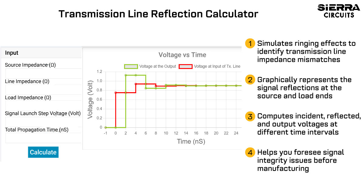
Sierra Circuits Transmission Line Reflection Calculator graphically displays the ringing of a signal in the transmission line.| Sierra Circuits
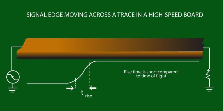
High clock frequencies and decreased rise times are some of the effects of high-speed signals in a PCB design, leading to signal degradation.| Sierra Circuits
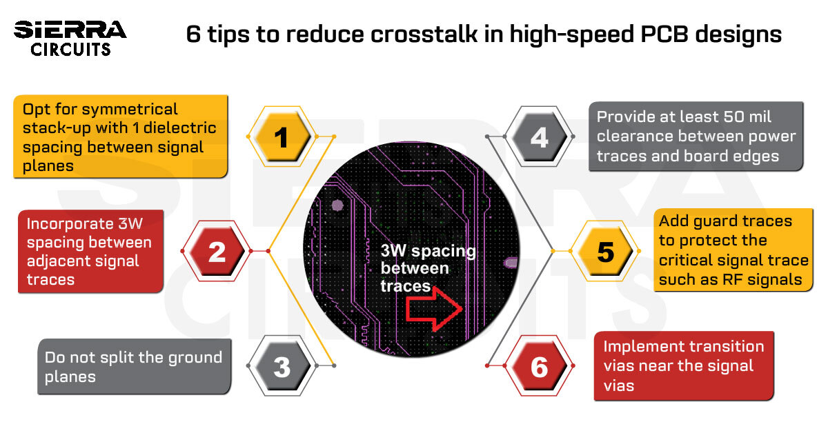
Crosstalk can be reduced in high-speed PCB designs by implementing 3W spacing between signal lines, guard traces, and solid ground planes.| Sierra Circuits
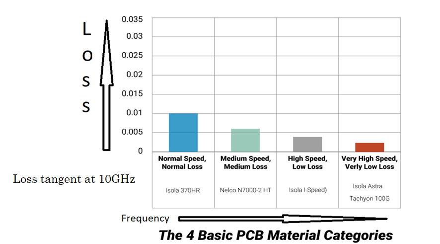
Proper PCB material selection is important since it affects the electrical performance of the signal traces.| Sierra Circuits
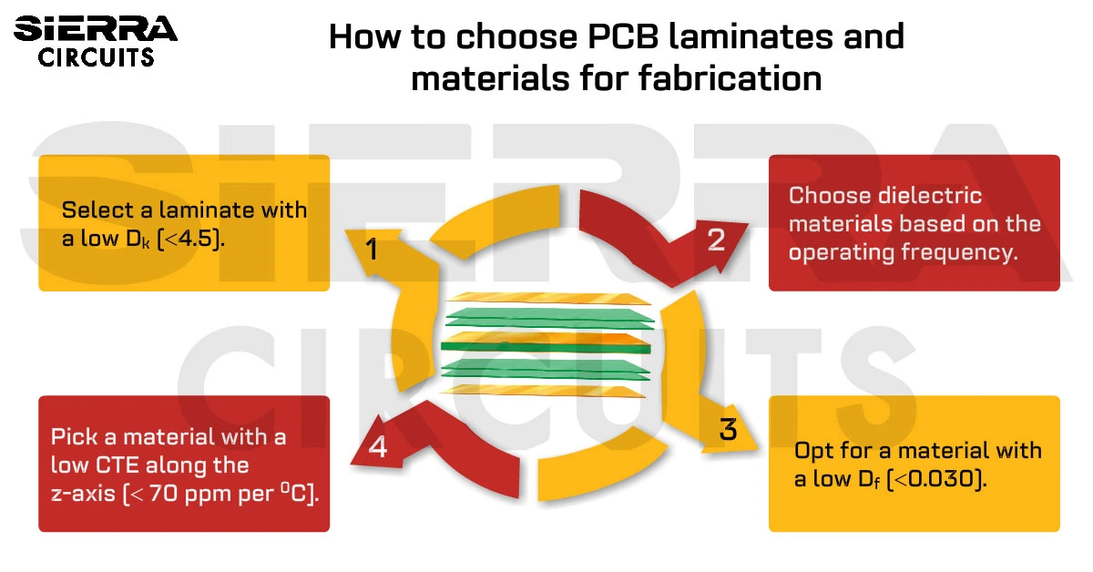
Selecting the right PCB laminates and materials for your design is very important as it can impact the overall performance of the board.| Sierra Circuits
FR4 materials are widely used due to their cost-effectiveness, wide range of operating temperatures, and excellent thermal properties.| Sierra Circuits
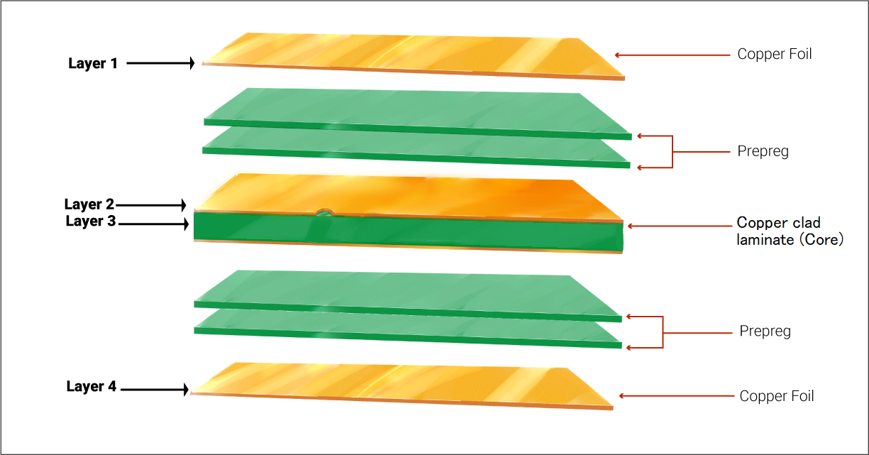
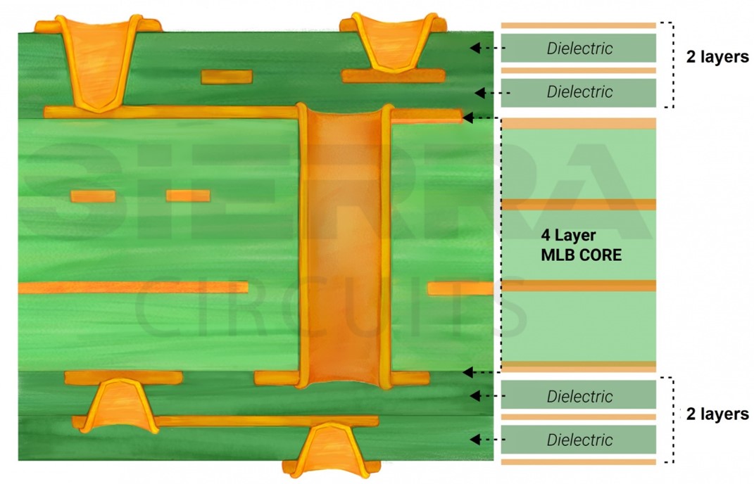
A multilayer PCB has more than two layers in its stack-up. The stack-up describes the construction of a multilayer board in sequential order.| Sierra Circuits
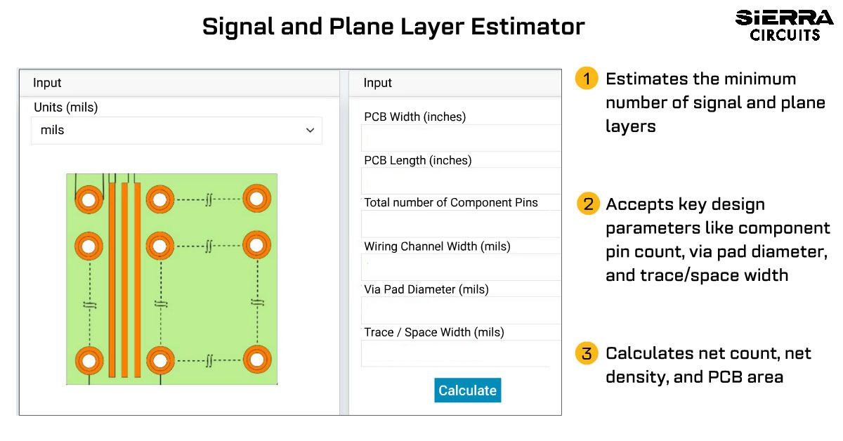
Try this easy-to-use PCB signal and plane layer estimator based on parameters like dimensions, component pin numbers, via pad diameters, etc.| Sierra Circuits
Download the High-Speed PCB Design Guide to design PCBs with signal frequencies from 50MHz to as high as 3GHz and beyond.| Sierra Circuits
Vias are miniature conductive pathways drilled into the PCB to establish electrical connectivity between the different layers.| Sierra Circuits
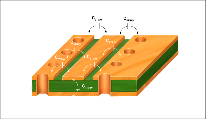
Parasitic capacitance effect in PCBs results in EMI and crosstalk. It can be reduced by following good layout practices.| Sierra Circuits
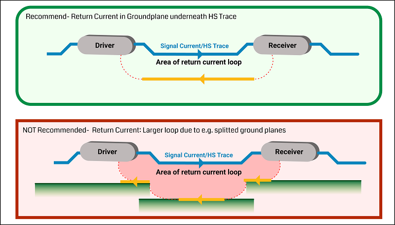
In high-speed PCBs, the current return path follows the path of least impedance instead of least resistance. The current always comes back to the source.| Sierra Circuits
