Effects of High-Speed Signals in PCB Design | Sierra Circuits
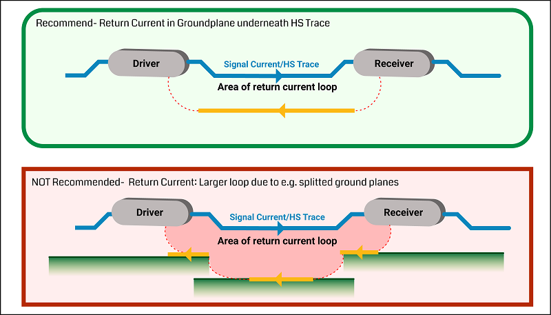
High clock frequencies and decreased rise times are some of the effects of high-speed signals in a PCB design, leading to signal degradation.| Sierra Circuits
High clock frequencies and decreased rise times are some of the effects of high-speed signals in a PCB design, leading to signal degradation.| Sierra Circuits

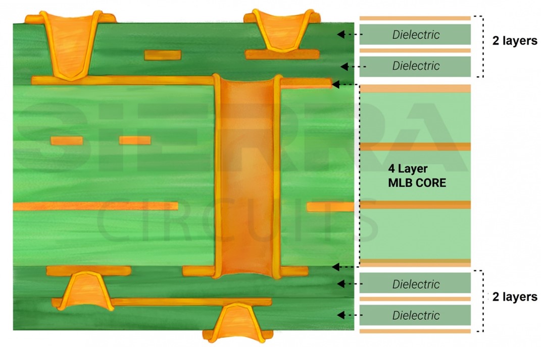
To build an efficient PCB stack-up, select the right materials, estimate the number of signal layers, and optimally arrange the layers.| Sierra Circuits
Vias are miniature conductive pathways drilled into the PCB to establish electrical connectivity between the different layers.| Sierra Circuits
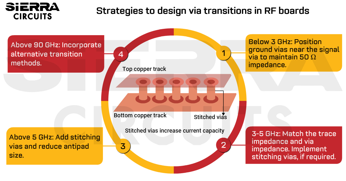
When designing RF PCB vias, ensure uniform impedance and consider parasitic effects, controlled impedance, and ground via placement.| Sierra Circuits
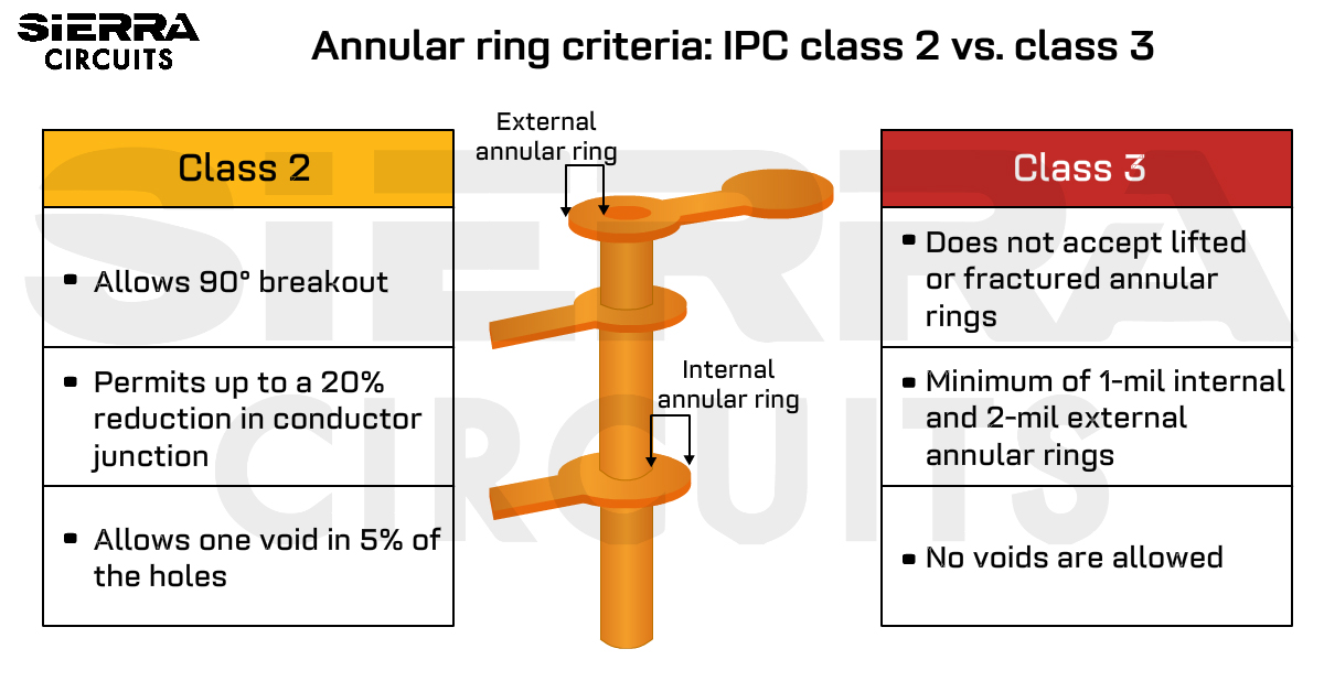
This article will help you understand the different PCB design rules for IPC Class 2 and Class 3 printed circuit boards.| Sierra Circuits
