How to Set Up Design Rules in KiCad | Sierra Circuits
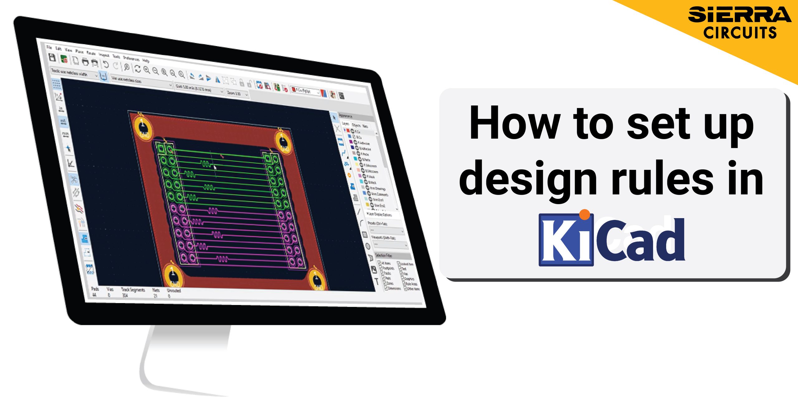
In this tutorial, you'll learn how to set up design rules in KiCad, such as trace width, clearance, via size, and net classes.| Sierra Circuits
In this tutorial, you'll learn how to set up design rules in KiCad, such as trace width, clearance, via size, and net classes.| Sierra Circuits
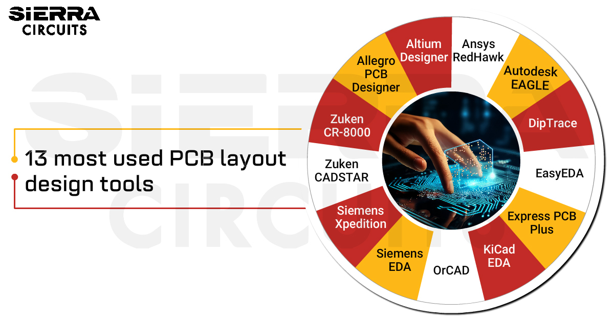
Some of the most used PCB layout design tools are Altium, Allegro, and KiCad. Consider UI, routing, and simulation before selecting one.| Sierra Circuits
Sierra Circuits Canada was established in 2022 to service the PCB manufacturing and assembly needs of our Canadian and worldwide customers.| Sierra Circuits
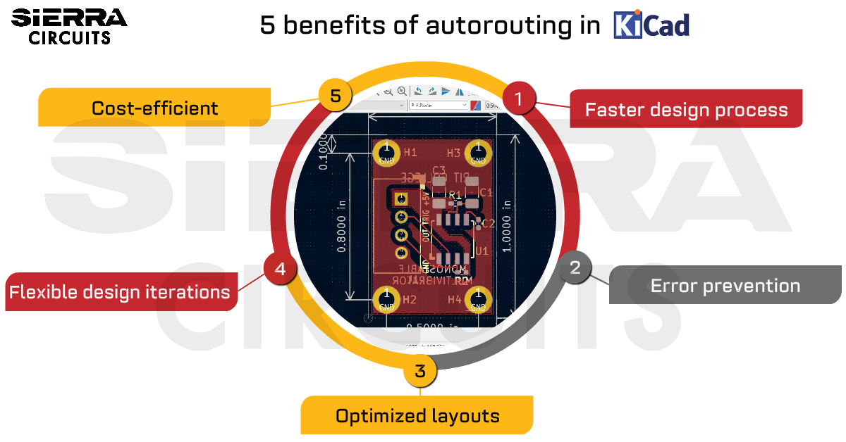
The autorouting plugin in KiCad automates the PCB routing process by creating optimized signal paths, improving the quality of your layouts.| Sierra Circuits
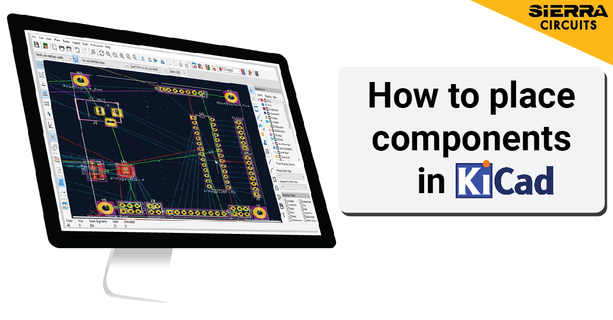
In this KiCad tutorial, you'll learn how to place components on your PCB layout and define your board outline.| Sierra Circuits
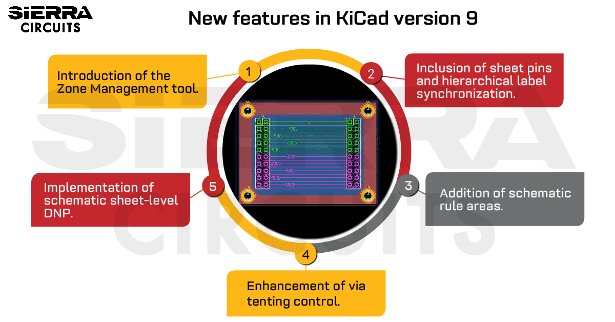
KiCad version 9 is set to add features like the new zone manager, sheet pin and label synchronization, and schematic sheet-level DNP.| Sierra Circuits
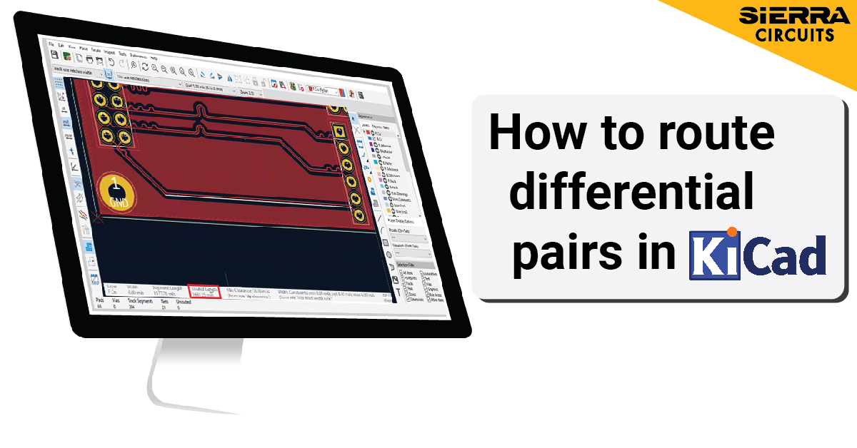
In this KiCad tutorial, you'll learn how to route differential pairs, fine-tune lengths, and manage skew to ensure signal integrity.| Sierra Circuits

In this KiCad tutorial, you will learn how to export IPC-2581, Gerber, and other production files such as drill files, netlist and BOM.| Sierra Circuits
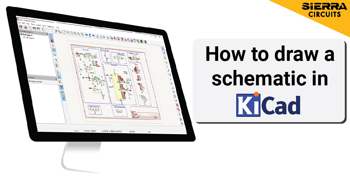
In this KiCad tutorial, you will learn how to create a schematic and build a custom symbol library from scratch.| Sierra Circuits
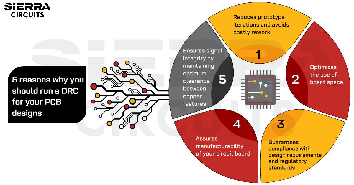
DRC helps you validate whether your PCB layout conforms to predefined constraints such as trace width, clearances, and hole sizes.| Sierra Circuits
