9 Factors that Cause Signal Integrity Issues | Sierra Circuits
Avoiding signal integrity issues in a PCB is a complex task for designers. It requires a deep understanding of design rules and techniques.| Sierra Circuits
Avoiding signal integrity issues in a PCB is a complex task for designers. It requires a deep understanding of design rules and techniques.| Sierra Circuits
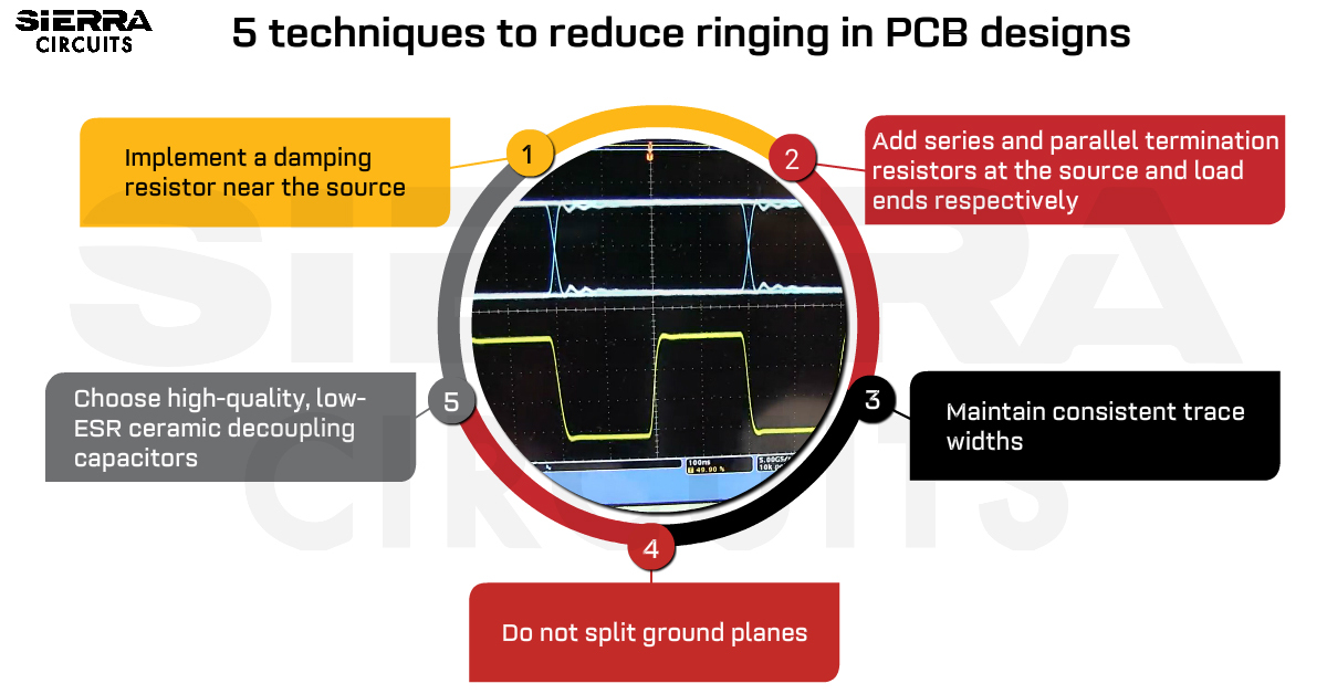
To reduce PCB ringing, implement a damping resistor at the source and maintain uniform trace width and spacing throughout the signal line.| Sierra Circuits
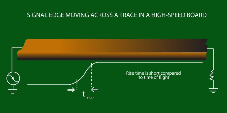
High clock frequencies and decreased rise times are some of the effects of high-speed signals in a PCB design, leading to signal degradation.| Sierra Circuits
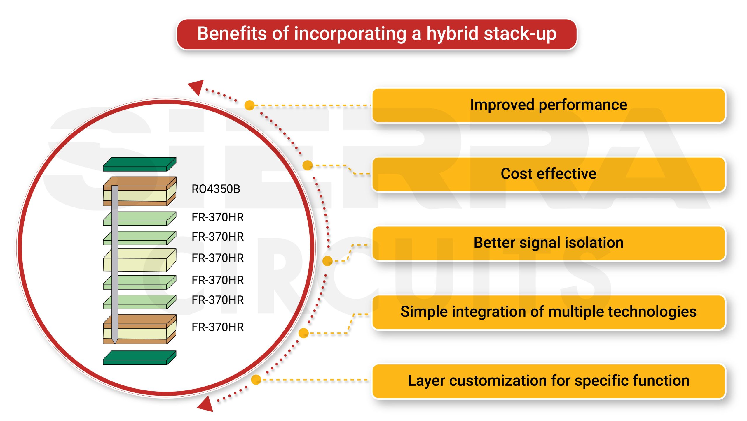
A hybrid stackup is built using a combination of dielectric materials to improve the PCB's performance and cost-effectiveness.| Sierra Circuits
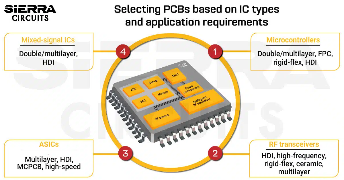
Selecting the right PCBs for IC integration depends on the chip’s signal characteristics, power demands, and the end-product.| Sierra Circuits
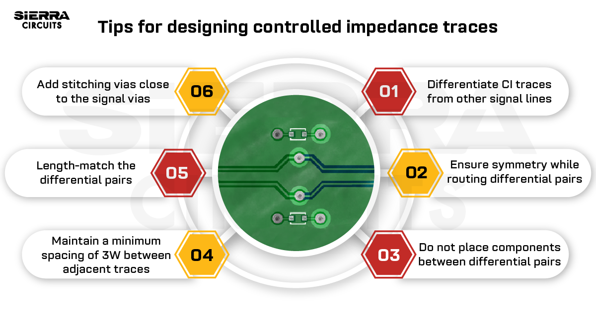
PCB materials, dielectric constant, trace height, and width affect the controlled impedance of a transmission line.| Sierra Circuits
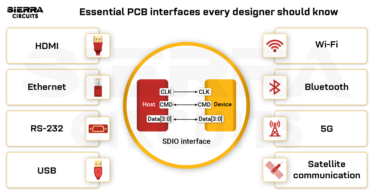
PCB interfaces are categorized into wired interfaces, like UART, I2C, and PCIe, and wireless interfaces, such as 5G, Wi-Fi, and LoRa.| Sierra Circuits
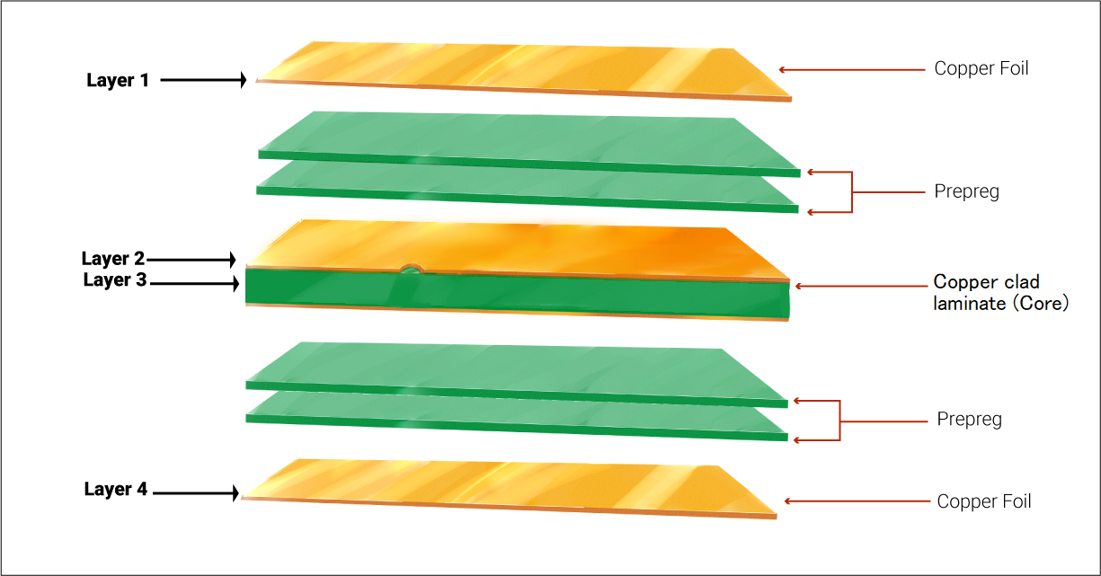
A multilayer PCB has more than two layers in its stack-up. The stack-up describes the construction of a multilayer board in sequential order.| Sierra Circuits
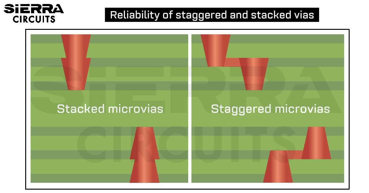
Staggered and stacked vias play crucial role in designing HDI boards. The compact design is highly functional with great signal integrity.| Sierra Circuits
Here are some best high-speed PCB routing practices that will help PCB designers to craft a perfect design.| Sierra Circuits
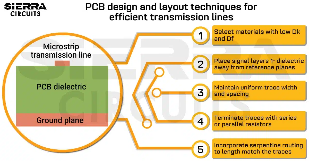
When designing PCB transmission lines, terminate the traces accurately and maintain a uniform trace width and spacing.| Sierra Circuits
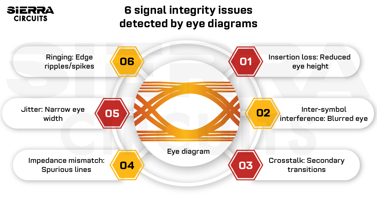
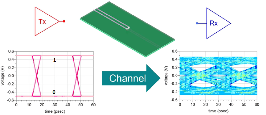
Eye diagrams reveal critical signal integrity issues like Inter-symbol interference, jitter, crosstalk, ringing, and reflections.| Sierra Circuits
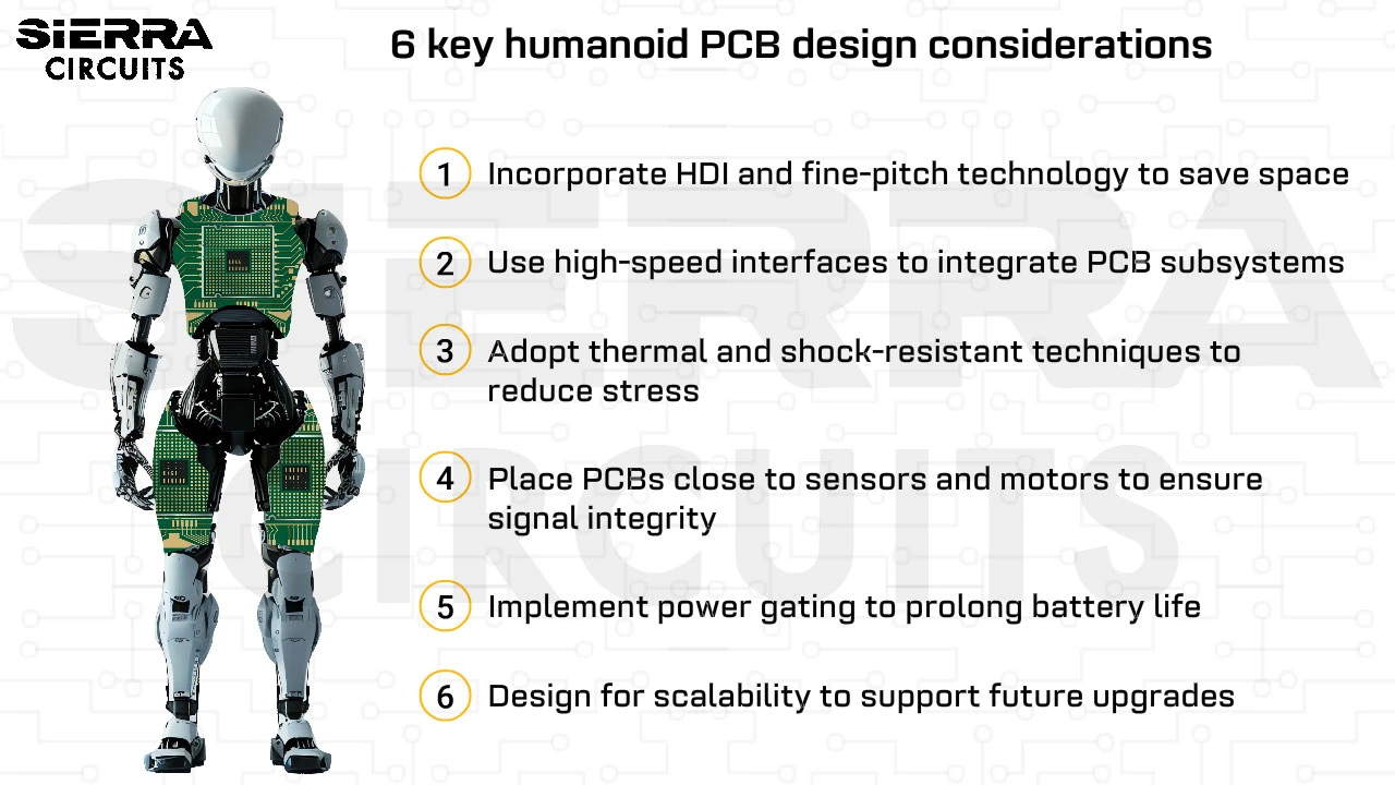
When designing humanoid robotics PCBs, use high-frequency materials and incorporate FPCs to integrate sensors.| Sierra Circuits
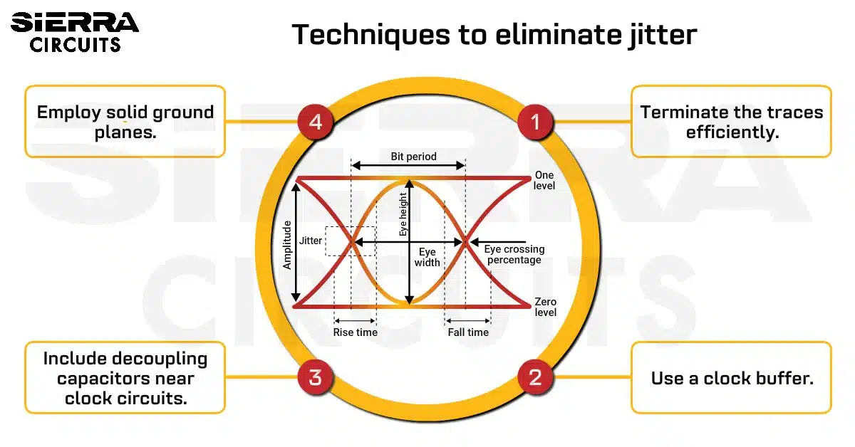
To avoid jitter in PCBs, terminate the traces efficiently and incorporate decoupling capacitors near clock drivers and receivers.| Sierra Circuits
Signal integrity is the measurement of a signal’s quality when it propagates from the transmitter to the receiver in an electronic system.| Sierra Circuits
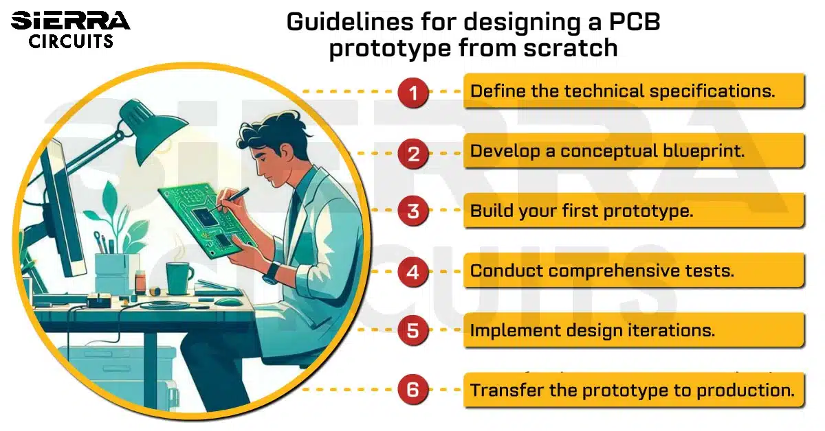
Designing a PCB prototype involves defining specifications, developing the system, testing, iterating, and validating with EVT samples.| Sierra Circuits
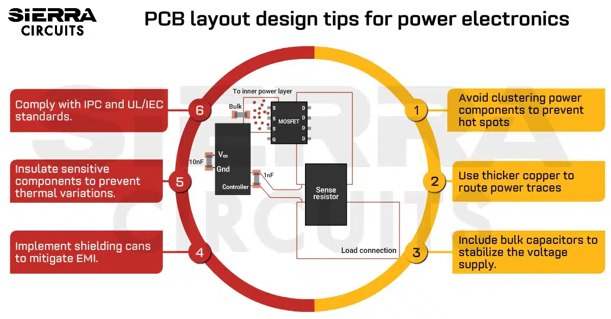
When designing a power electronics PCB, pick high thermal conductivity materials, integrate protection devices, and adhere to IPC standards.| Sierra Circuits
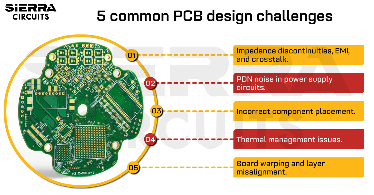
Learn the solutions for 5 common PCB design challenges like impedance discontinuities, EMI, crosstalk, part overlap, and PDN noise.| Sierra Circuits

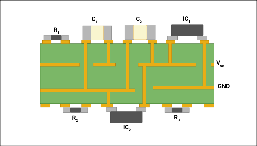
PCB fabrication considerations for proper component placement are essential to improve the signal quality and performance of your device.| Sierra Circuits
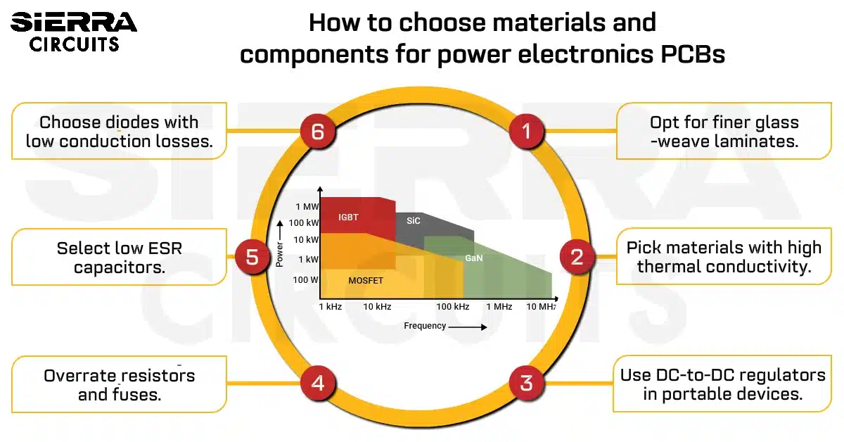
Effective component selection for power electronics PCBs focuses on low-loss diodes, low ESR capacitors, and low DCR inductors.| Sierra Circuits
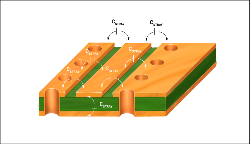
Parasitic capacitance effect in PCBs results in EMI and crosstalk. It can be reduced by following good layout practices.| Sierra Circuits
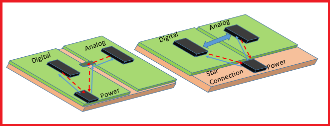
Understanding the operating range of frequencies is critical for decoupling capacitor placement to avoid EMI and EMC issues.| Sierra Circuits
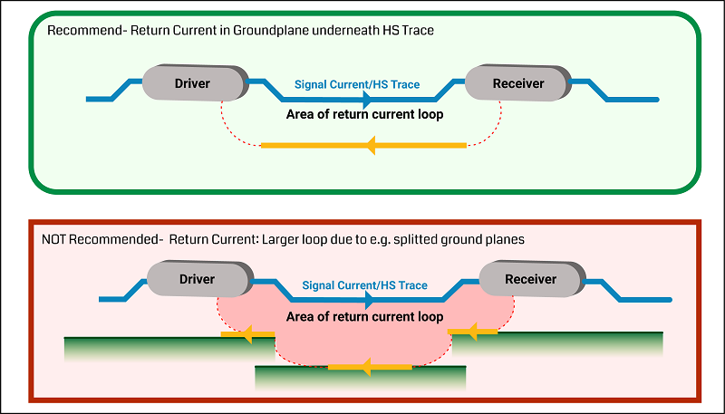
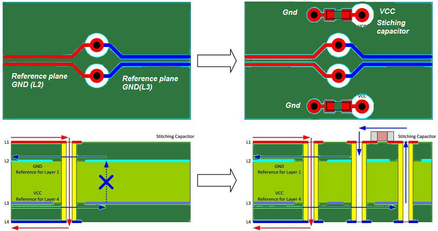
In high-speed PCBs, the current return path follows the path of least impedance instead of least resistance. The current always comes back to the source.| Sierra Circuits
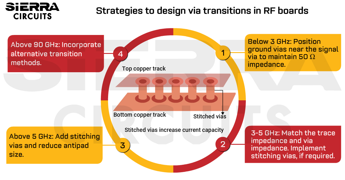
When designing RF PCB vias, ensure uniform impedance and consider parasitic effects, controlled impedance, and ground via placement.| Sierra Circuits
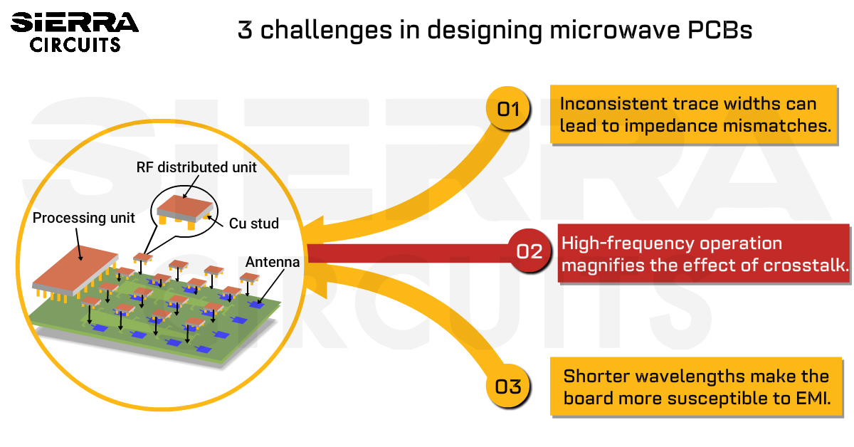
To design a microwave PCB, select materials with low dielectric constant, prefer CPWs, and add board-level shielding to mitigate EMI effects.| Sierra Circuits
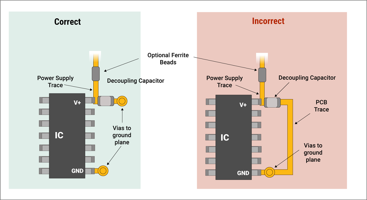
Placement of a decoupling capacitor or bypass capacitor is critical as it provides high transient currents to an IC to reduce power ripples.| Sierra Circuits
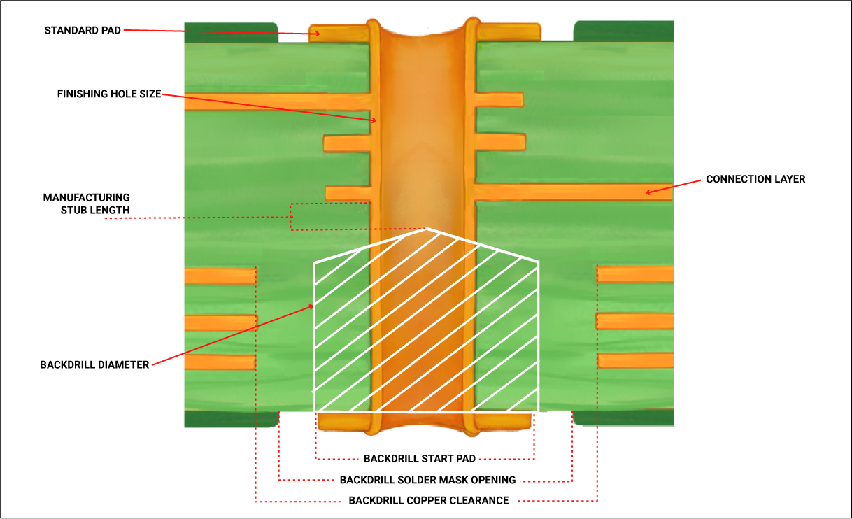
Back drilling in PCB involves drilling a hole slightly larger in diameter than the PTH to remove the conductive via stub.| Sierra Circuits
