OhmegaPly and TCR with Embedded Passives | Sierra Circuits
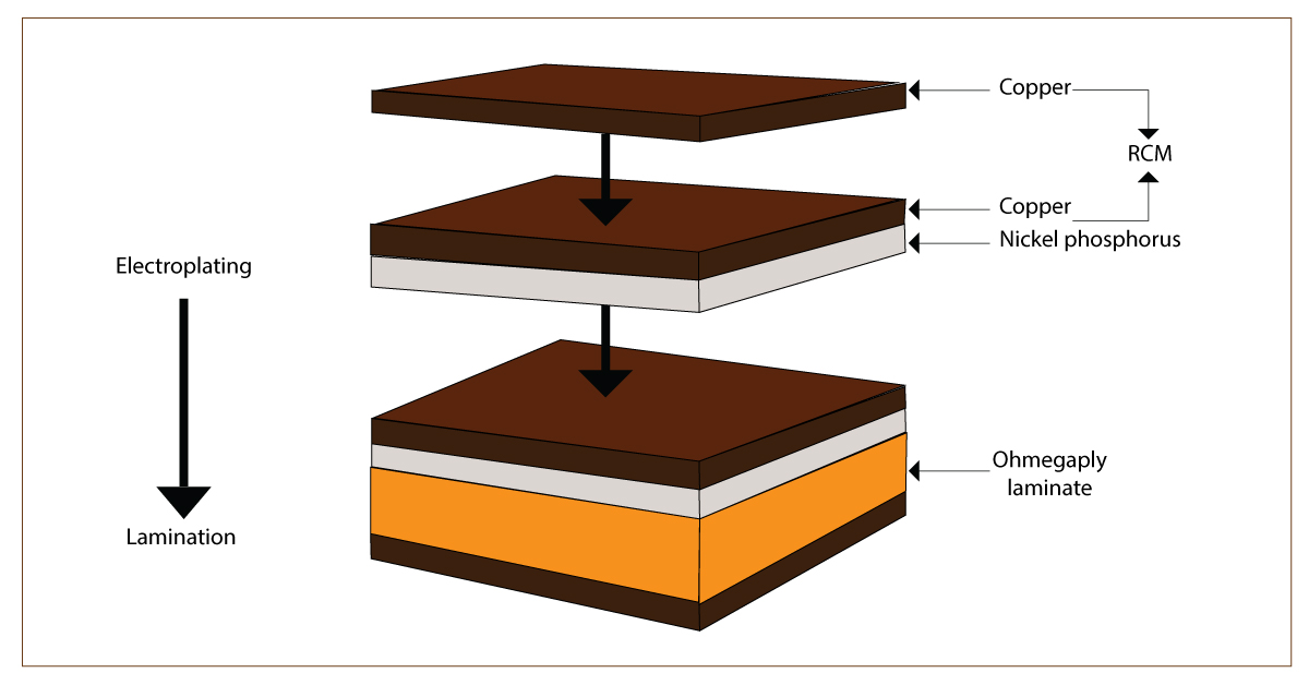
OhmegaPly and TCR follow the embedded passives technology that manufactures components like resistors and capacitors into the PCB substrate.| Sierra Circuits
OhmegaPly and TCR follow the embedded passives technology that manufactures components like resistors and capacitors into the PCB substrate.| Sierra Circuits
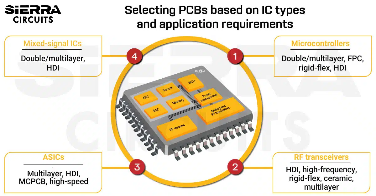
Selecting the right PCBs for IC integration depends on the chip’s signal characteristics, power demands, and the end-product.| Sierra Circuits
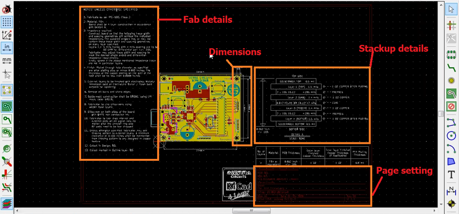
A PCB fab drawing is a reference document for manufacturing and includes all the information like board outline, stack-up, drilled holes, etc.| Sierra Circuits
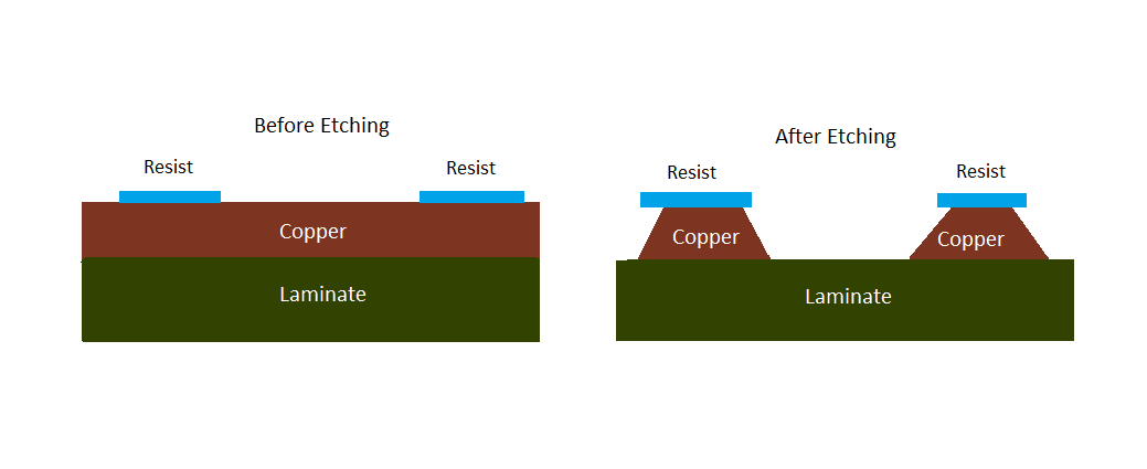
Wet PCB etching is a process of removing unwanted copper by immersing a circuit board in a chemical solution (acidic or alkaline based).| Sierra Circuits

PCB fabrication considerations for proper component placement are essential to improve the signal quality and performance of your device.| Sierra Circuits
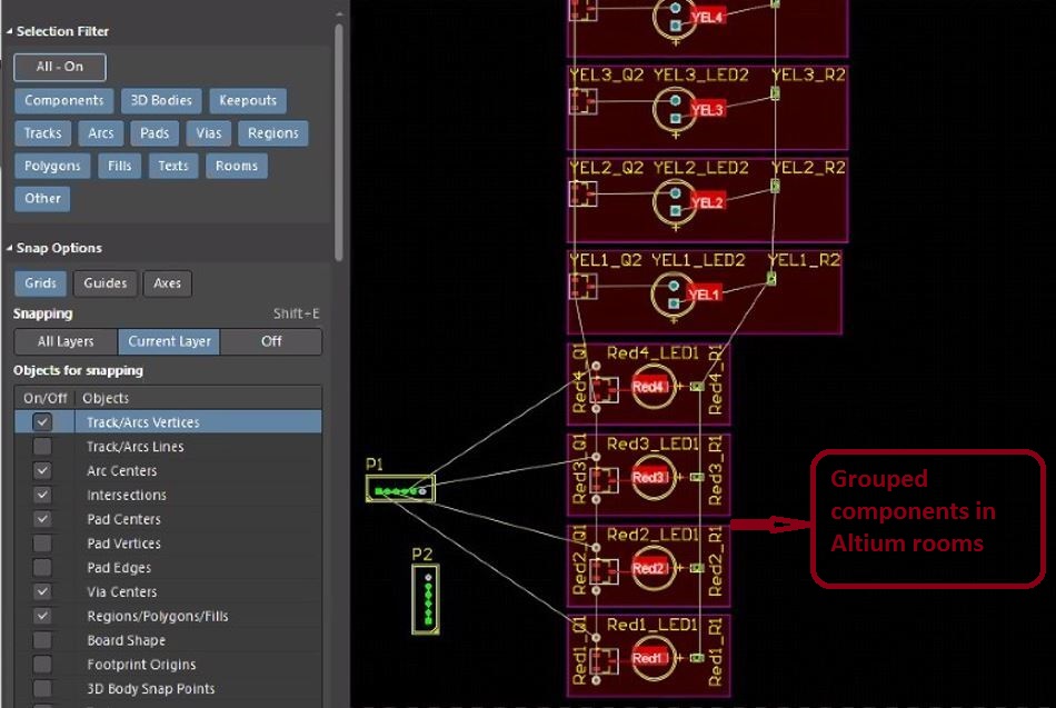
Auto grouping of repetitive PCB design blocks is essential to reduce the overall time consumption and complexity of your board layout.| Sierra Circuits
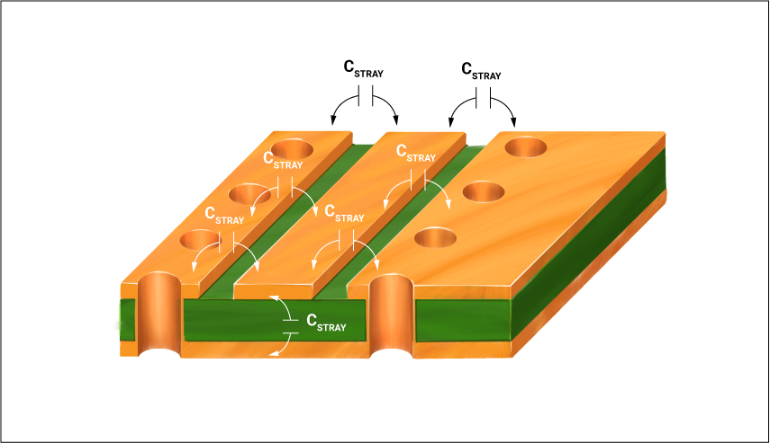
Parasitic capacitance effect in PCBs results in EMI and crosstalk. It can be reduced by following good layout practices.| Sierra Circuits
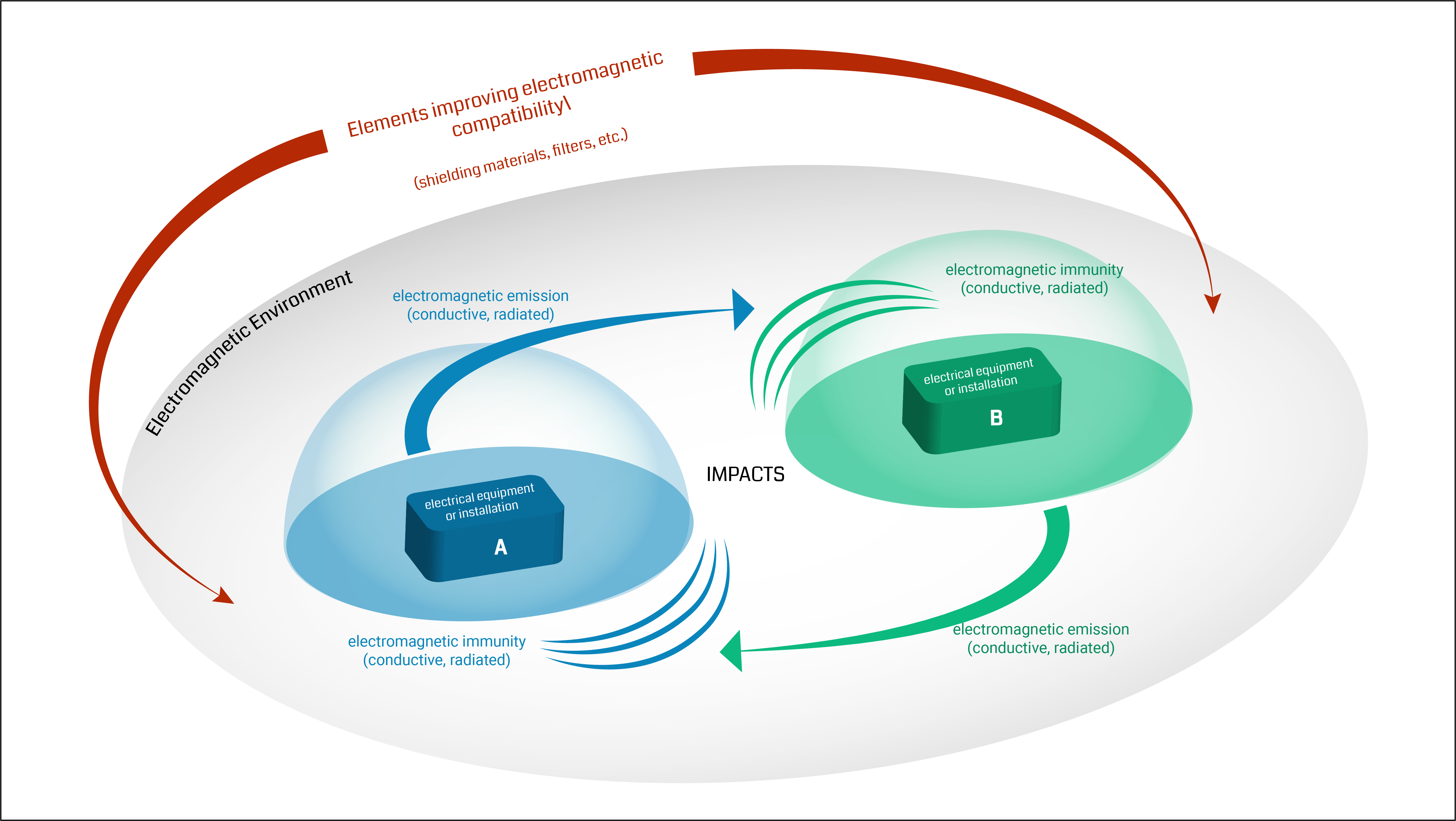
EMI can be mitigated by incorporating efficient grounding techniques and optimum trace spacing. This also ensures EMC.| Sierra Circuits
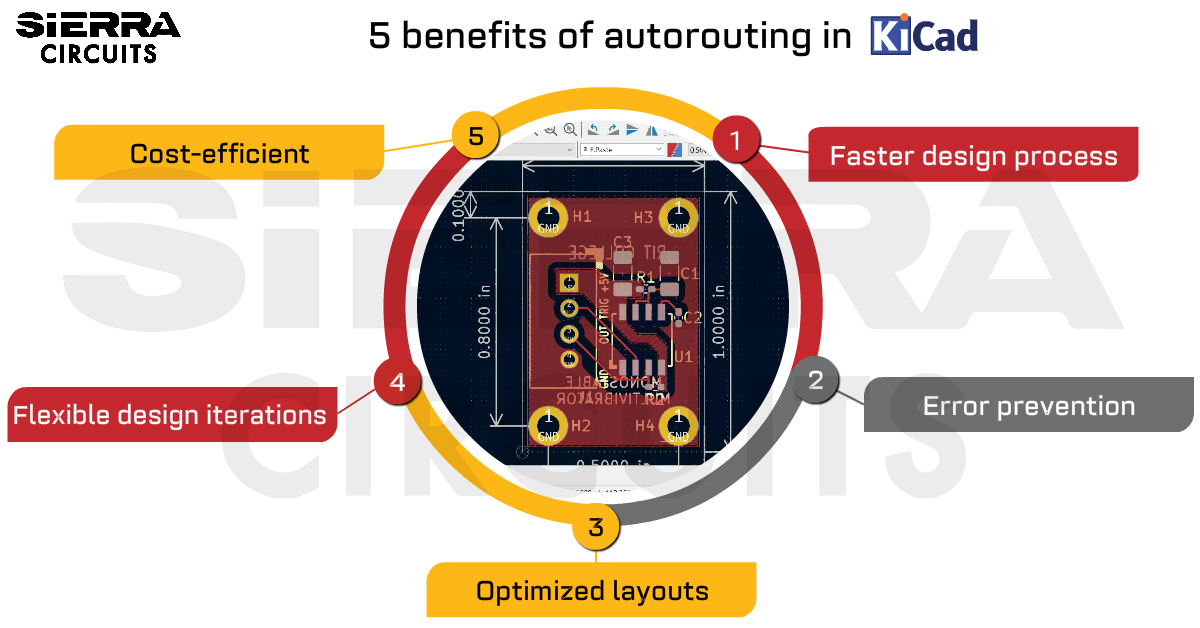
The autorouting plugin in KiCad automates the PCB routing process by creating optimized signal paths, improving the quality of your layouts.| Sierra Circuits
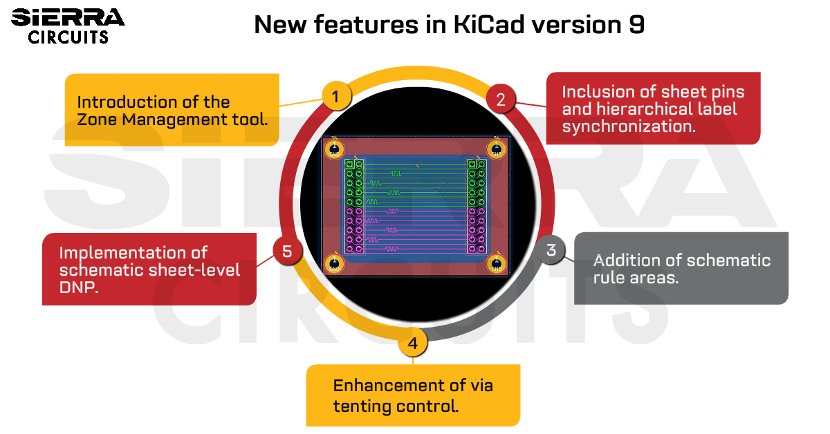
KiCad version 9 is set to add features like the new zone manager, sheet pin and label synchronization, and schematic sheet-level DNP.| Sierra Circuits

A PCB bill of materials (BOM) is a comprehensive list that provides information on all the components to be assembled on your board.| Sierra Circuits
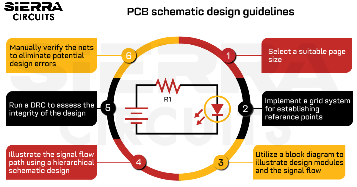
A PCB schematic must follow standard guidelines such as precision net labeling, and symbol standardization to have a well-structured design.| Sierra Circuits
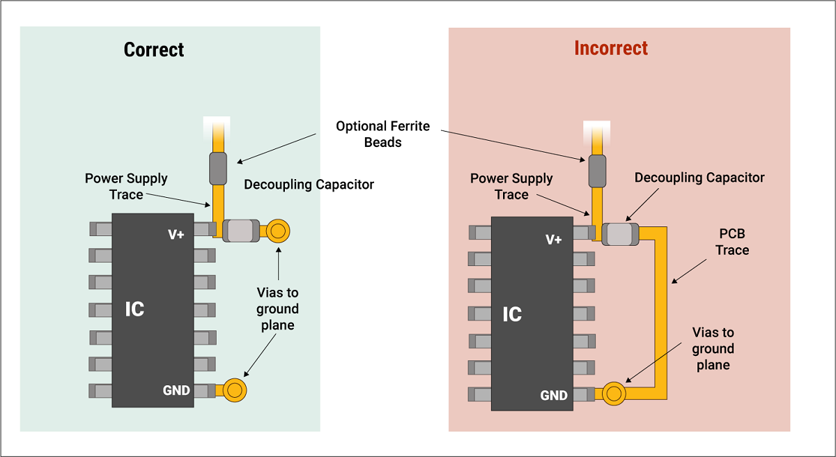
Placement of a decoupling capacitor or bypass capacitor is critical as it provides high transient currents to an IC to reduce power ripples.| Sierra Circuits
