9 Factors that Cause Signal Integrity Issues | Sierra Circuits
Avoiding signal integrity issues in a PCB is a complex task for designers. It requires a deep understanding of design rules and techniques.| Sierra Circuits
Avoiding signal integrity issues in a PCB is a complex task for designers. It requires a deep understanding of design rules and techniques.| Sierra Circuits
Signal attenuation is the measure of the reduction in signal strength. It can be controlled by adopting repeaters, amplifiers, and materials| Sierra Circuits
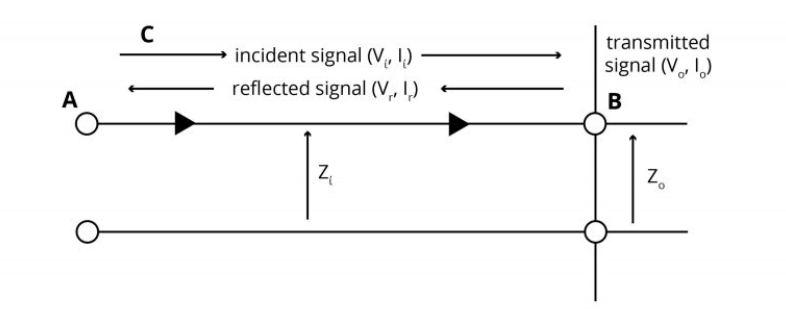
We previously discussed impedance discontinuity and signal reflection in our PCB transmission line series. Reflections occur due to impedance discontinuity.| Sierra Circuits
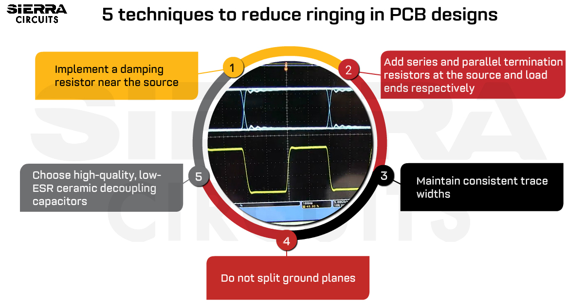
To reduce PCB ringing, implement a damping resistor at the source and maintain uniform trace width and spacing throughout the signal line.| Sierra Circuits
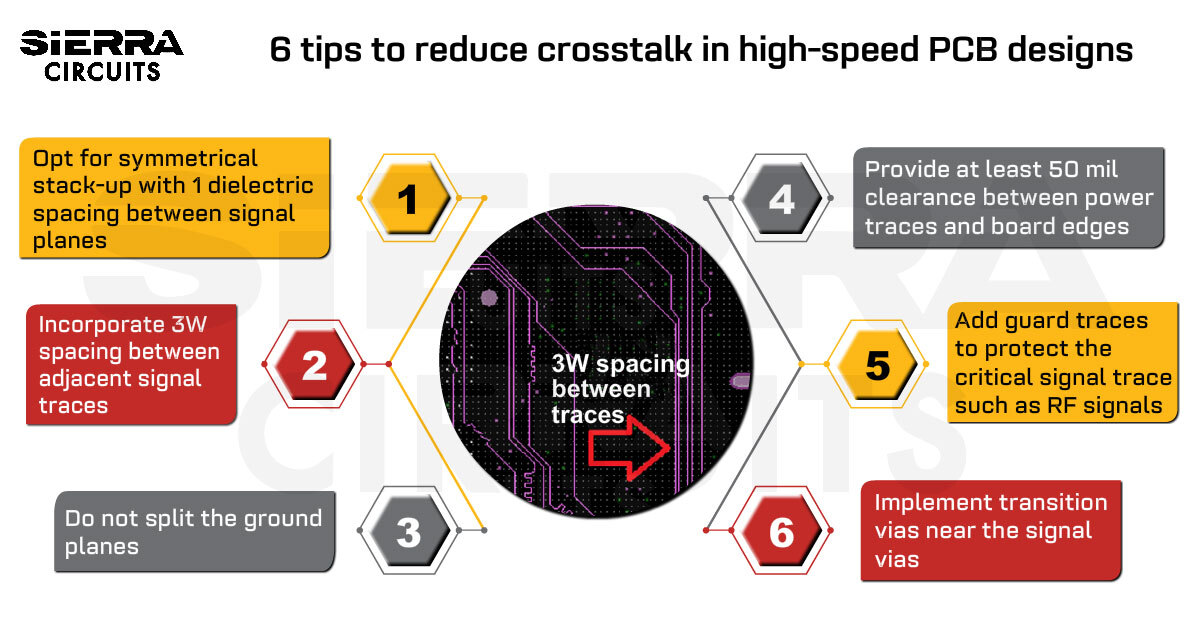
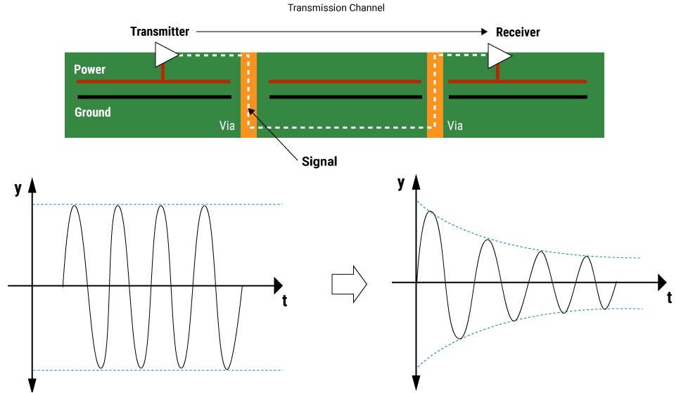
Crosstalk can be reduced in high-speed PCB designs by implementing 3W spacing between signal lines, guard traces, and solid ground planes.| Sierra Circuits
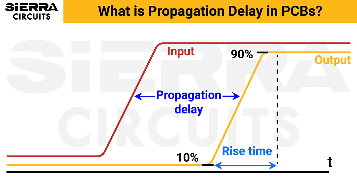
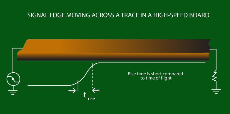
Propagation delay (tpd) in PCBs is the time taken by a signal to travel through a unit length of a transmission line.| Sierra Circuits
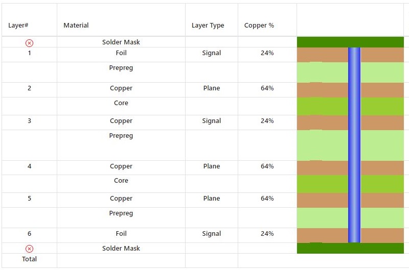
PCB layer count estimation is a critical step to achieving design success as it directly impacts the functional capability of your board.| Sierra Circuits
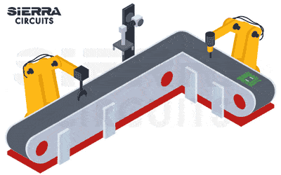
PCB assembly process involves DFA, SMT and through-hole components placement, testing, and final inspection.| Sierra Circuits
FR4 materials are widely used due to their cost-effectiveness, wide range of operating temperatures, and excellent thermal properties.| Sierra Circuits
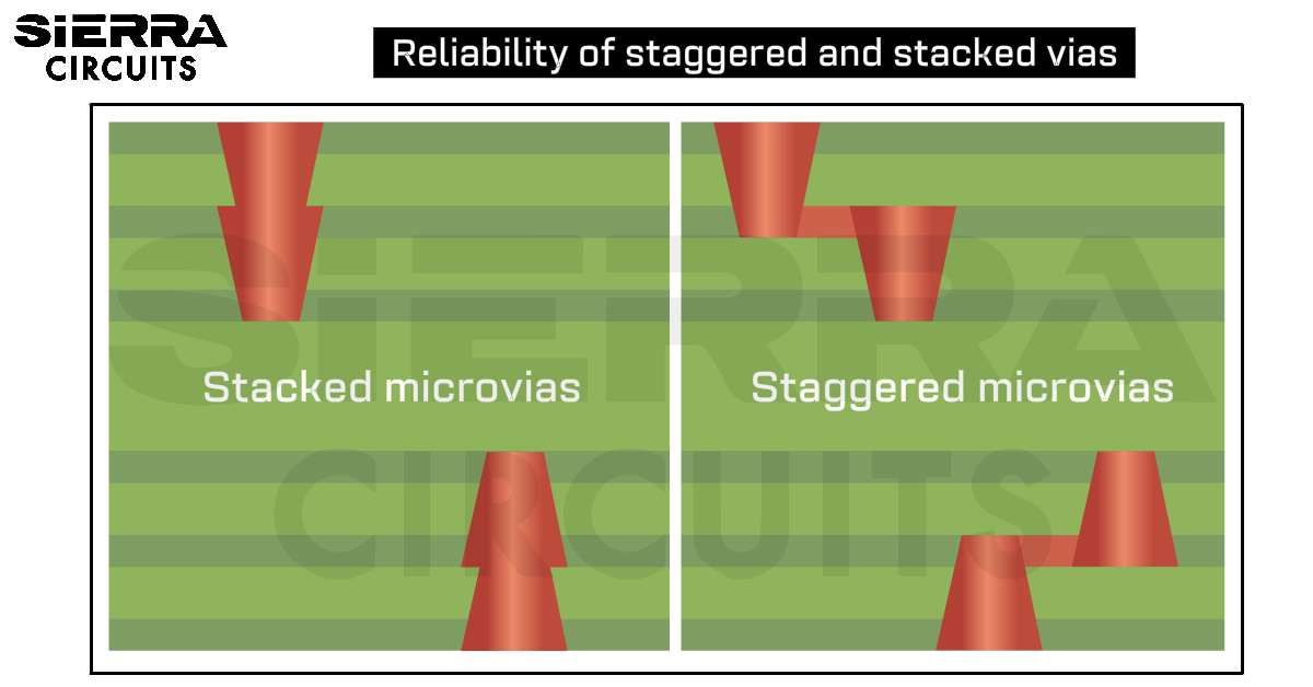
Staggered and stacked vias play crucial role in designing HDI boards. The compact design is highly functional with great signal integrity.| Sierra Circuits
Here are some best high-speed PCB routing practices that will help PCB designers to craft a perfect design.| Sierra Circuits
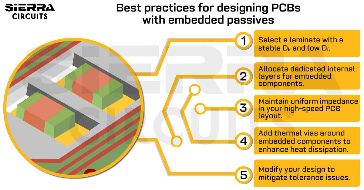
Embedded PCB components are passive devices fabricated within the PCB substrate. They reduce parasitic effects and enhance heat dissipation.| Sierra Circuits
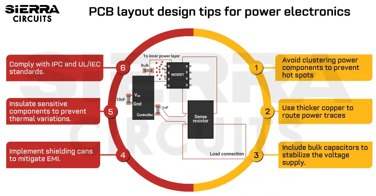
When designing a power electronics PCB, pick high thermal conductivity materials, integrate protection devices, and adhere to IPC standards.| Sierra Circuits
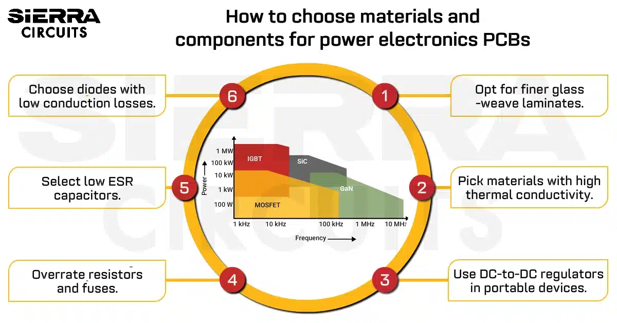
Effective component selection for power electronics PCBs focuses on low-loss diodes, low ESR capacitors, and low DCR inductors.| Sierra Circuits
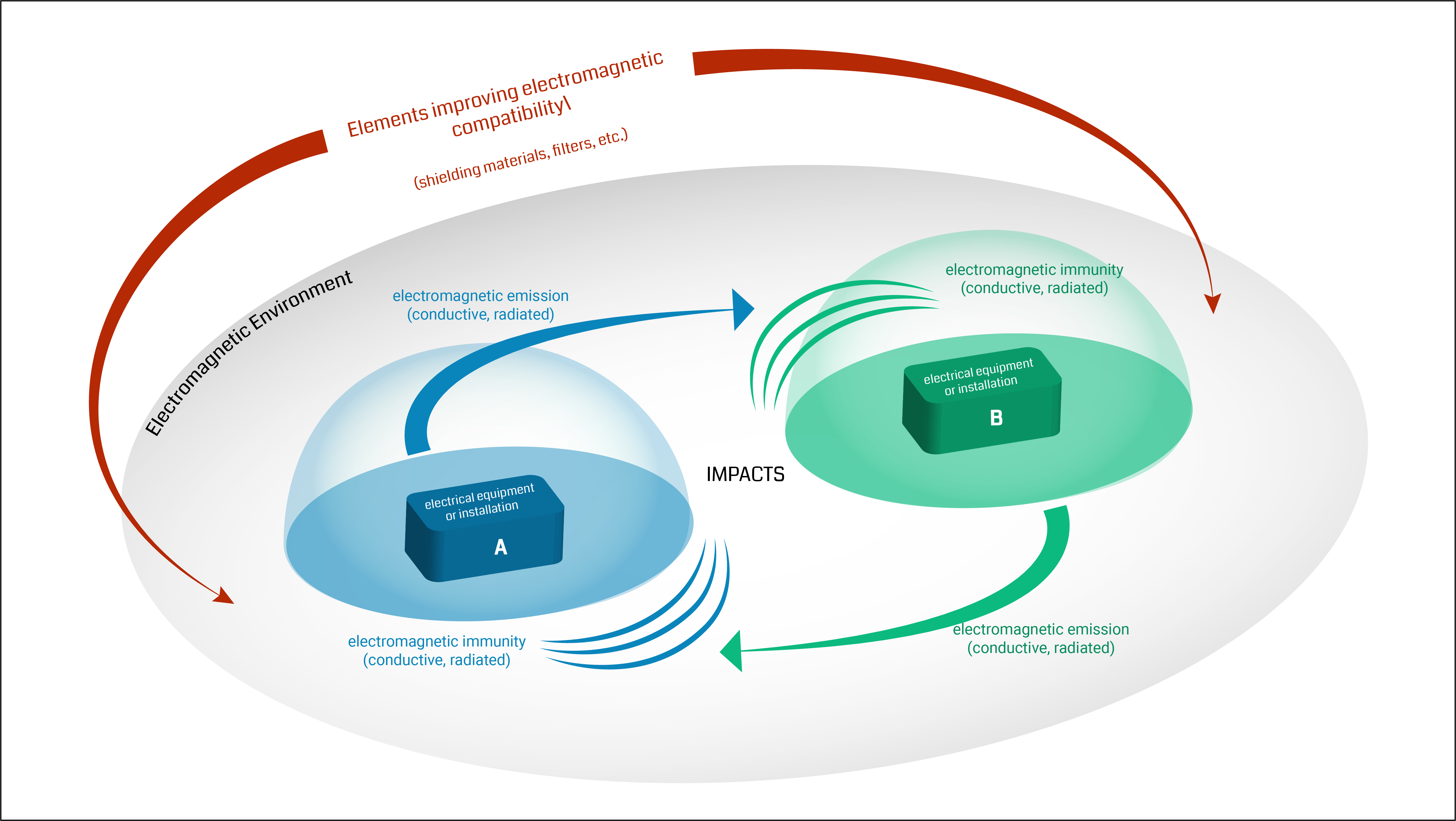
EMI can be mitigated by incorporating efficient grounding techniques and optimum trace spacing. This also ensures EMC.| Sierra Circuits
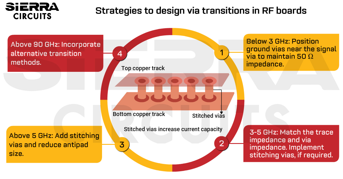
When designing RF PCB vias, ensure uniform impedance and consider parasitic effects, controlled impedance, and ground via placement.| Sierra Circuits
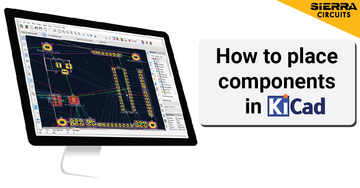
In this KiCad tutorial, you'll learn how to place components on your PCB layout and define your board outline.| Sierra Circuits
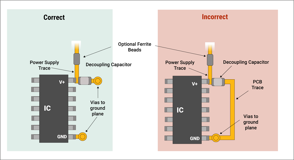
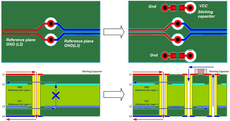
Placement of a decoupling capacitor or bypass capacitor is critical as it provides high transient currents to an IC to reduce power ripples.| Sierra Circuits
