PCB Via Design Using Altium Designer | Sierra Circuits
In this article, we will go over the fundamentals of via design using Altium Designer electronic design automation software.| Sierra Circuits
In this article, we will go over the fundamentals of via design using Altium Designer electronic design automation software.| Sierra Circuits
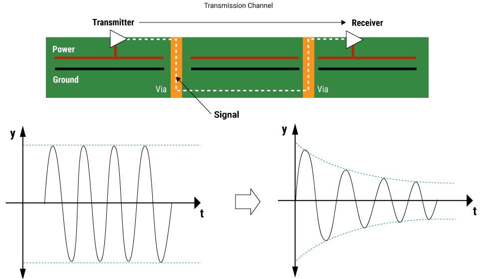
Signal attenuation is the measure of the reduction in signal strength. It can be controlled by adopting repeaters, amplifiers, and materials| Sierra Circuits
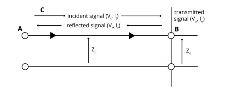
We previously discussed impedance discontinuity and signal reflection in our PCB transmission line series. Reflections occur due to impedance discontinuity.| Sierra Circuits
High clock frequencies and decreased rise times are some of the effects of high-speed signals in a PCB design, leading to signal degradation.| Sierra Circuits
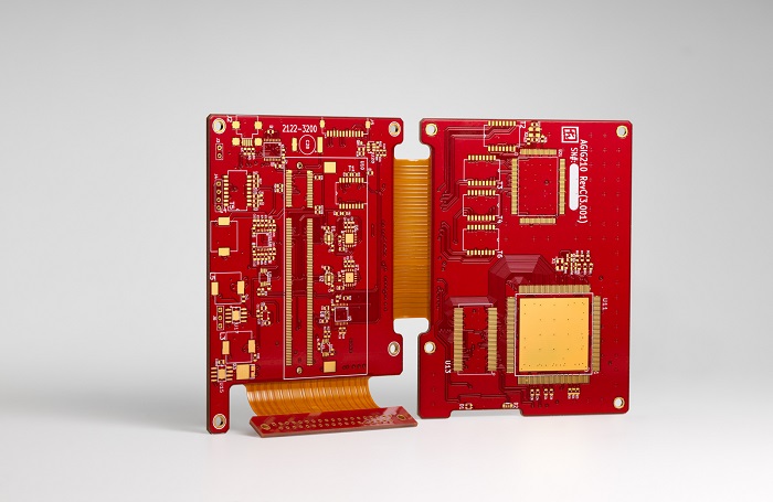
Rigid-flex PCB designs may be expensive to fabricate, but they can essentially save costs during electronic system assembly.| Sierra Circuits
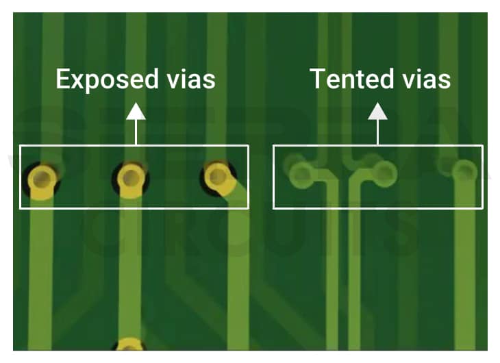
PCB via tenting protects vias from contamination, corrosion, and electrical shorts by covering exposed vias with a solder mask.| Sierra Circuits
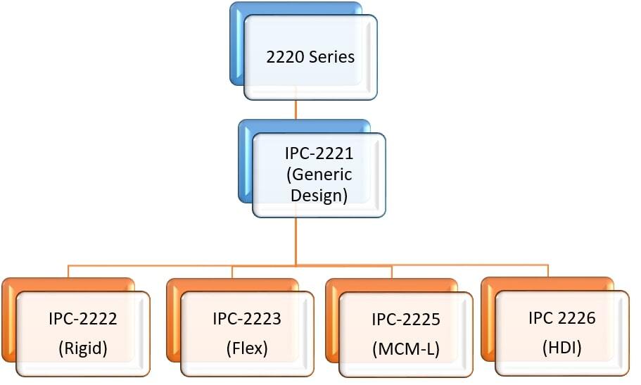
IPC-2221 is a standard that lays down the requirements for material selection, component placement, and high-voltage spacing requirements.| Sierra Circuits
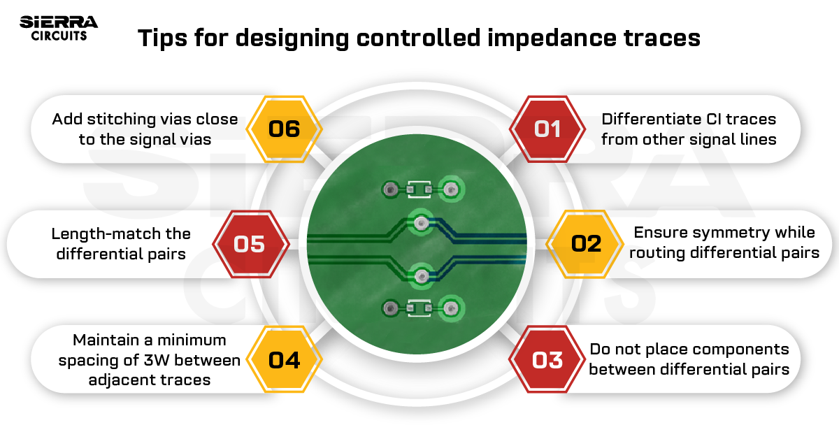
PCB materials, dielectric constant, trace height, and width affect the controlled impedance of a transmission line.| Sierra Circuits
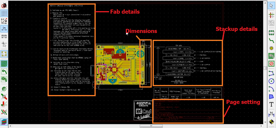
A PCB fab drawing is a reference document for manufacturing and includes all the information like board outline, stack-up, drilled holes, etc.| Sierra Circuits
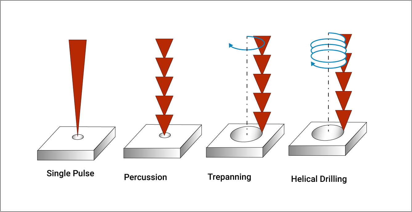
Laser drilling is performed to drill holes and vias on a PCB using a laser beam without compromising the board integrity.| Sierra Circuits
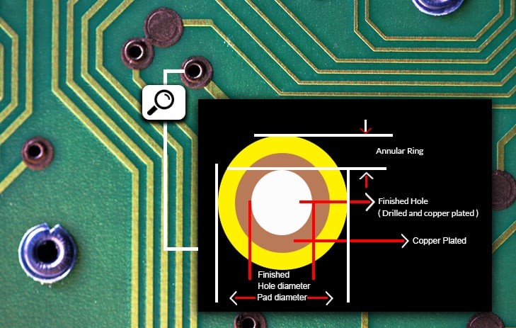
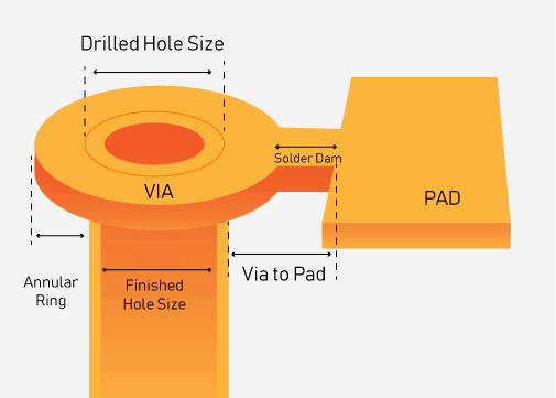
An annular ring is the copper area surrounding a plated via on a PCB. It establishes a solid connection between the via and copper traces.| Sierra Circuits
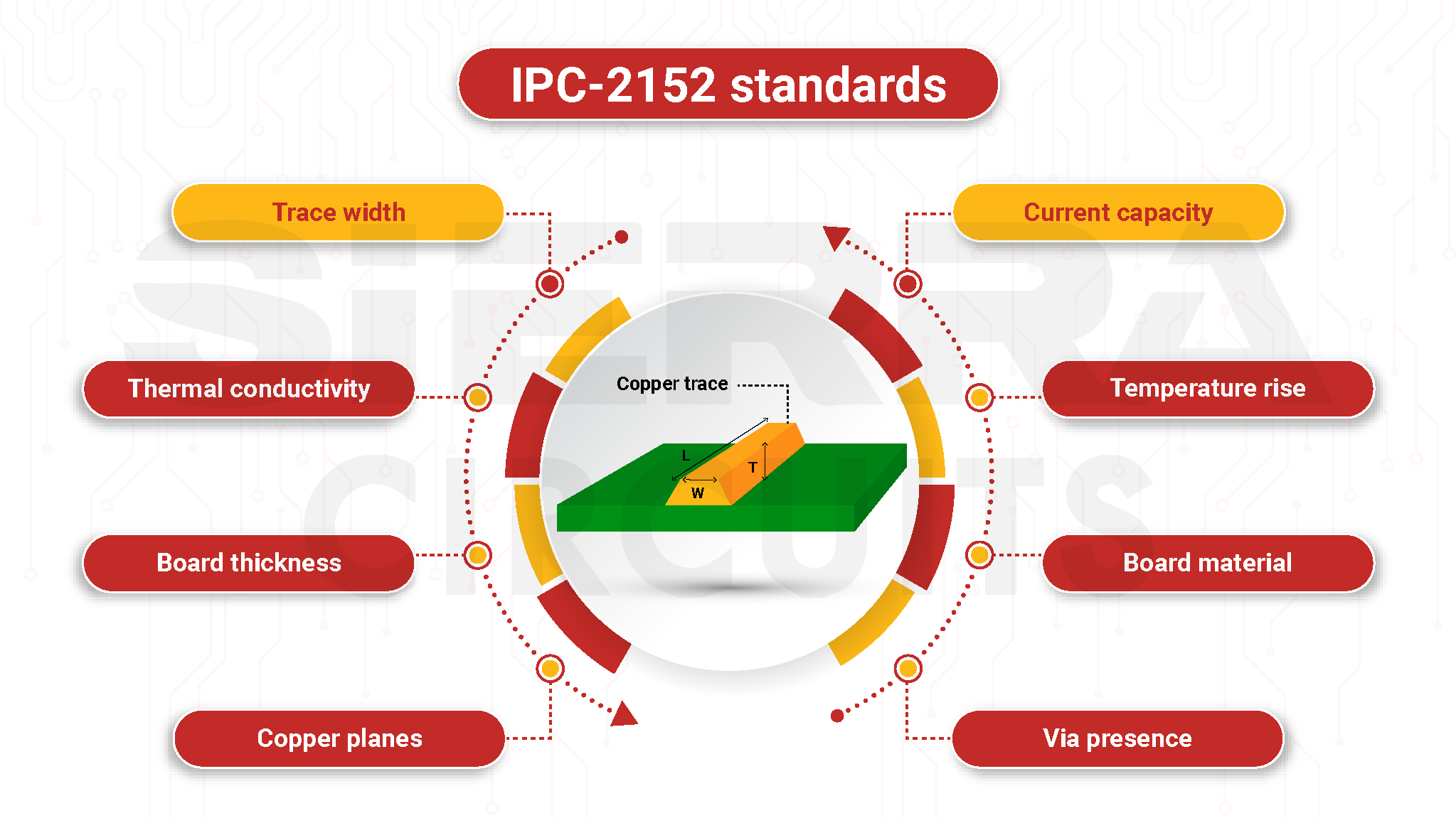
The IPC-2152 standard helps you optimize the current capacity, temperature rise, and width of a trace for efficient thermal management.| Sierra Circuits
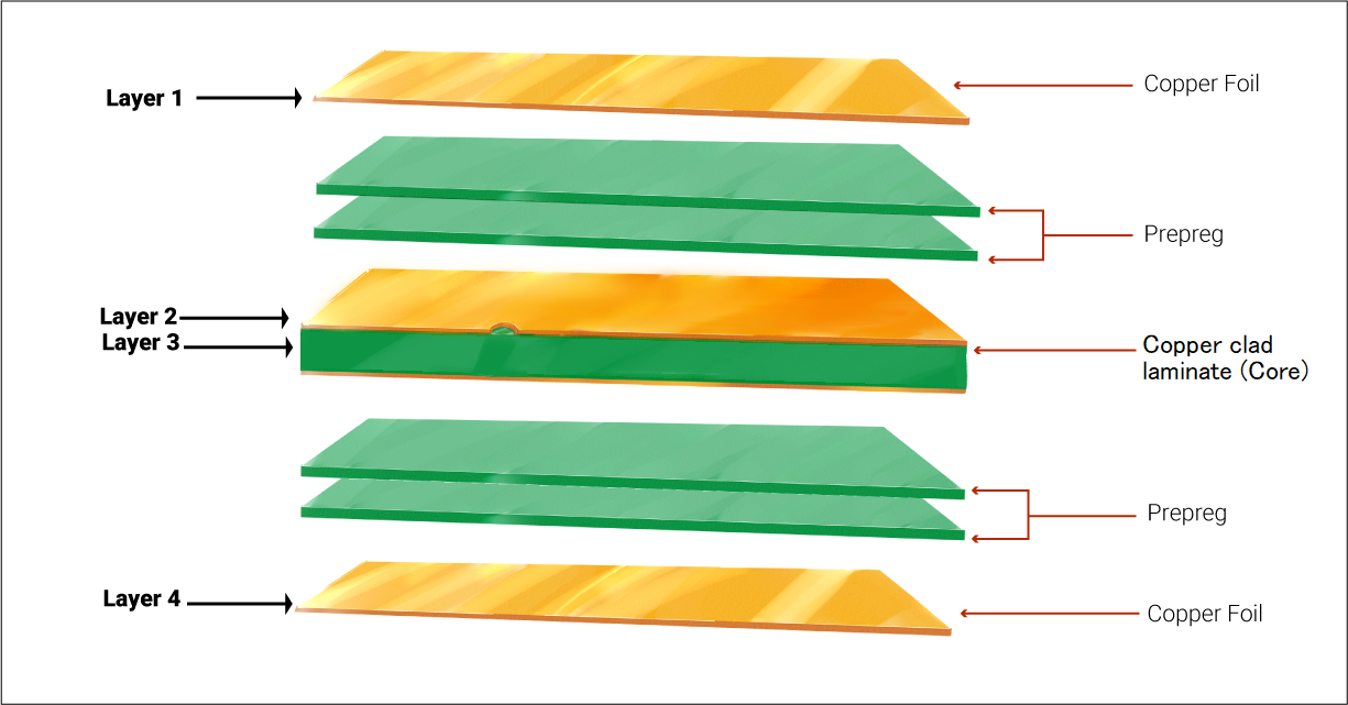
A multilayer PCB has more than two layers in its stack-up. The stack-up describes the construction of a multilayer board in sequential order.| Sierra Circuits
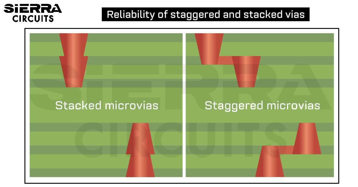
Staggered and stacked vias play crucial role in designing HDI boards. The compact design is highly functional with great signal integrity.| Sierra Circuits
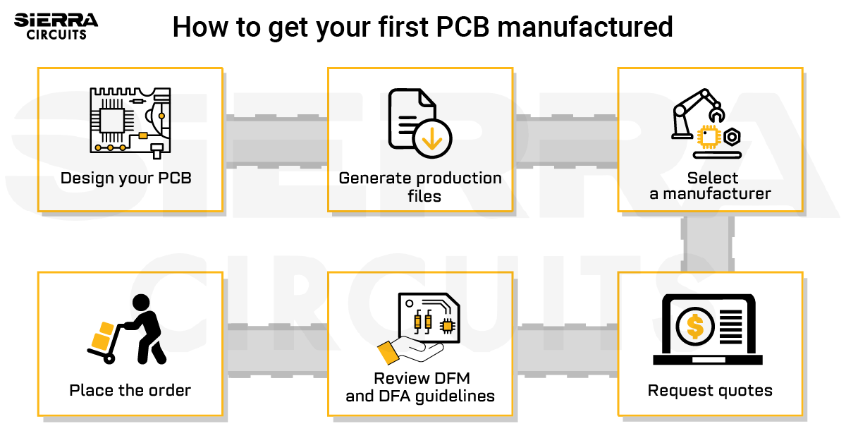
To get your first PCB manufactured, design your board, select a manufacturer, perform DFM and DFA analysis, and place the order.| Sierra Circuits
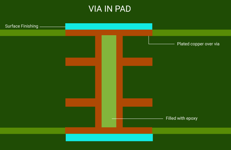
Use via-in-pad technology when the board size is limited, components have small footprints, and surface routing options are restricted.| Sierra Circuits
Drilling is the most expensive and time-consuming process in PCB manufacturing. A small fault in the drilling process leads to a great loss.| Sierra Circuits

PCB via current carrying capacity can be regulated using the process of tenting, plugging, and via current calculators.| Sierra Circuits
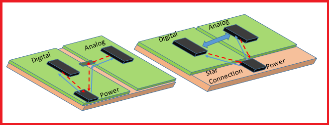
Employ decoupling capacitors, ferrite beads, and Faraday cages to suppress the power supply noise in your PDN design.| Sierra Circuits

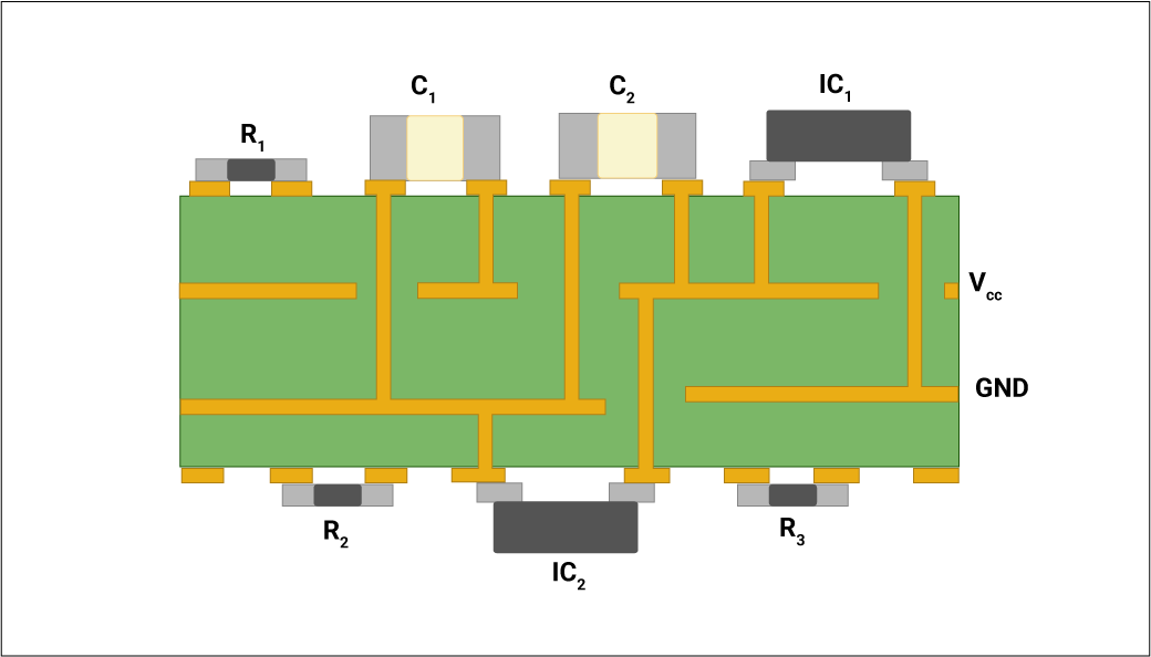
PCB fabrication considerations for proper component placement are essential to improve the signal quality and performance of your device.| Sierra Circuits
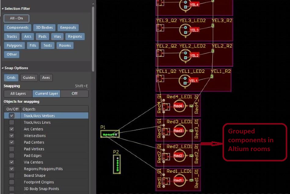
Auto grouping of repetitive PCB design blocks is essential to reduce the overall time consumption and complexity of your board layout.| Sierra Circuits
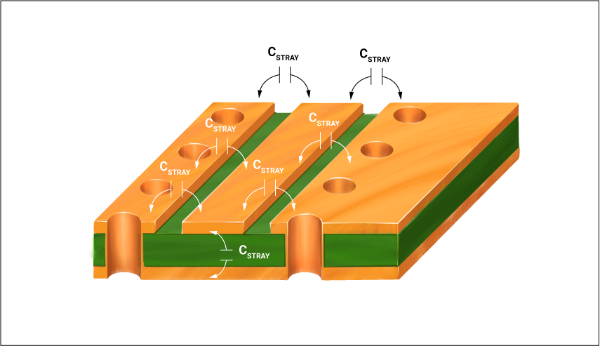
Parasitic capacitance effect in PCBs results in EMI and crosstalk. It can be reduced by following good layout practices.| Sierra Circuits
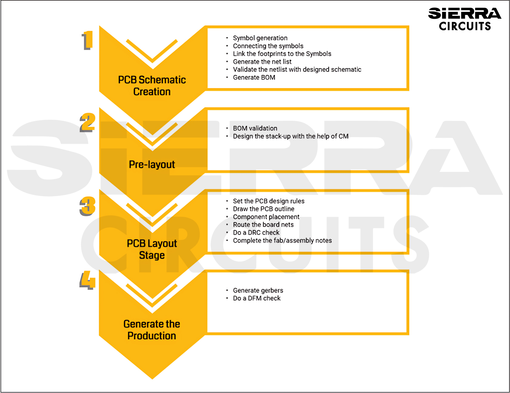
The PCB layout stage includes setting up the design tool, board outline, import of netlist, component placement, routing, silkscreen cleanup, and DRC check.| Sierra Circuits
Understanding the operating range of frequencies is critical for decoupling capacitor placement to avoid EMI and EMC issues.| Sierra Circuits
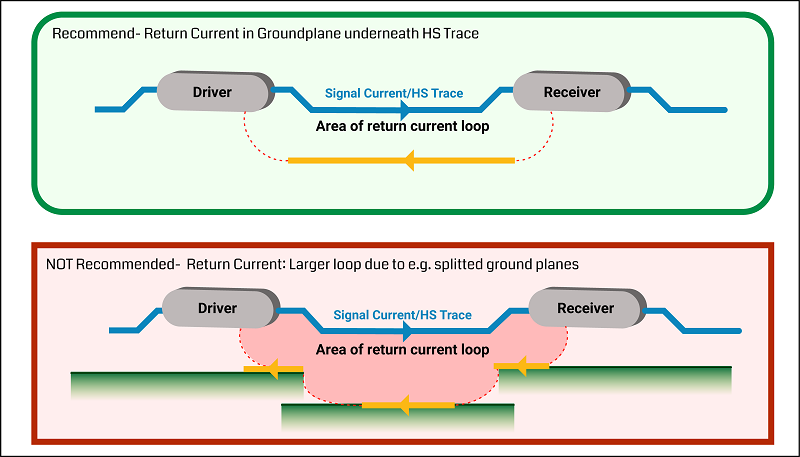
In high-speed PCBs, the current return path follows the path of least impedance instead of least resistance. The current always comes back to the source.| Sierra Circuits
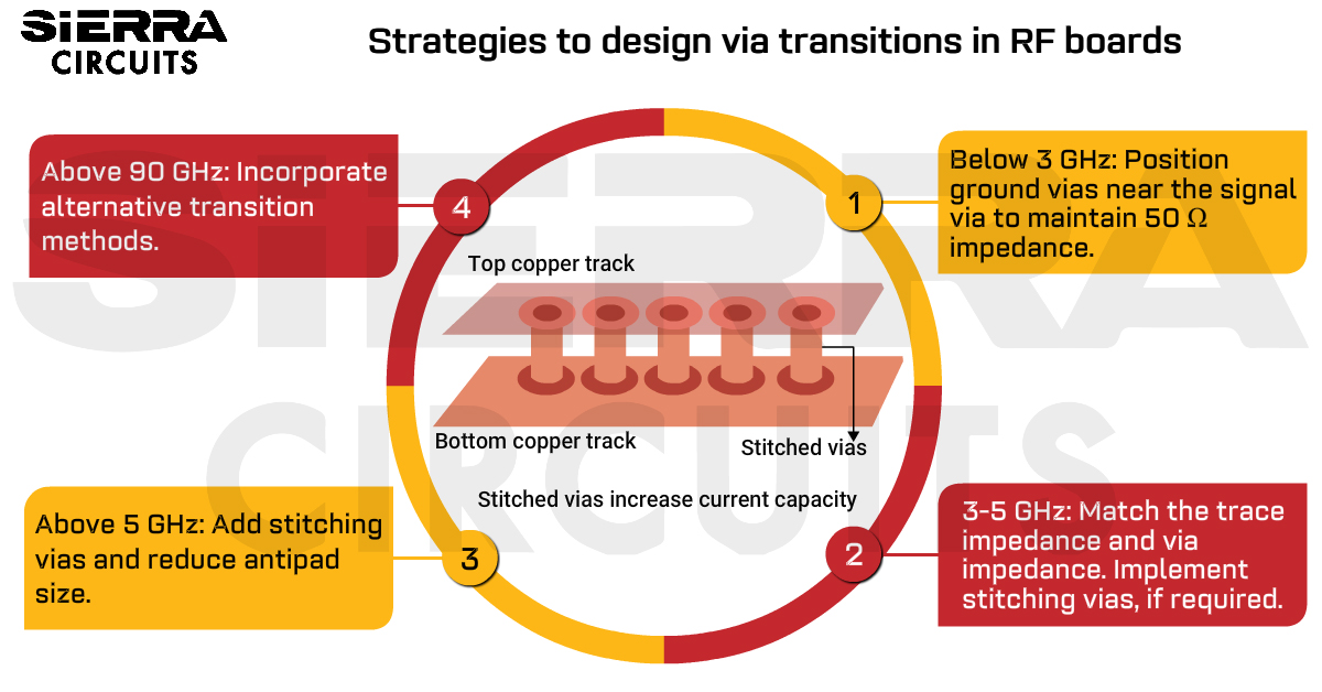
When designing RF PCB vias, ensure uniform impedance and consider parasitic effects, controlled impedance, and ground via placement.| Sierra Circuits
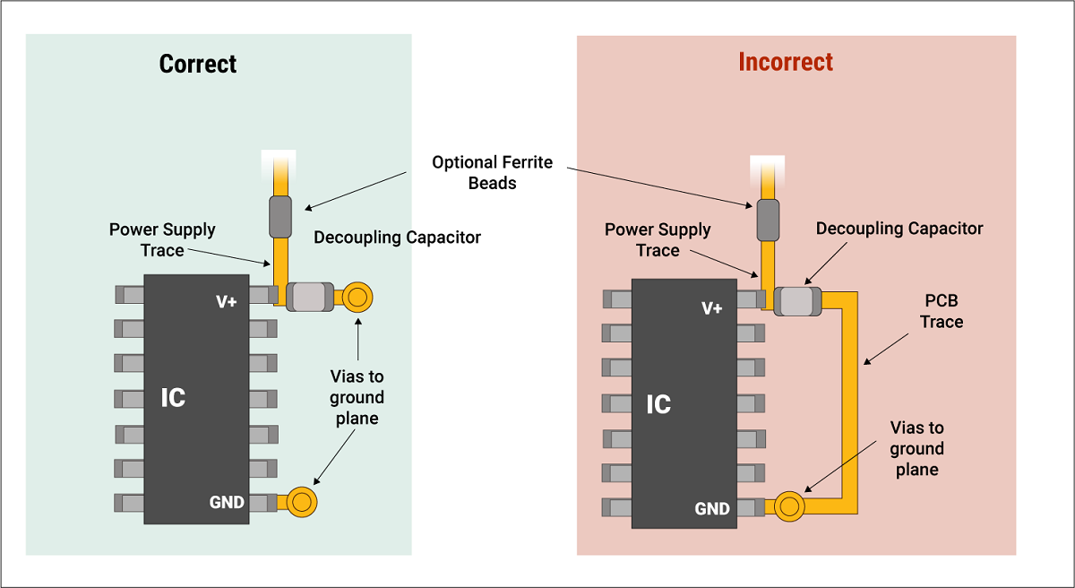
Placement of a decoupling capacitor or bypass capacitor is critical as it provides high transient currents to an IC to reduce power ripples.| Sierra Circuits
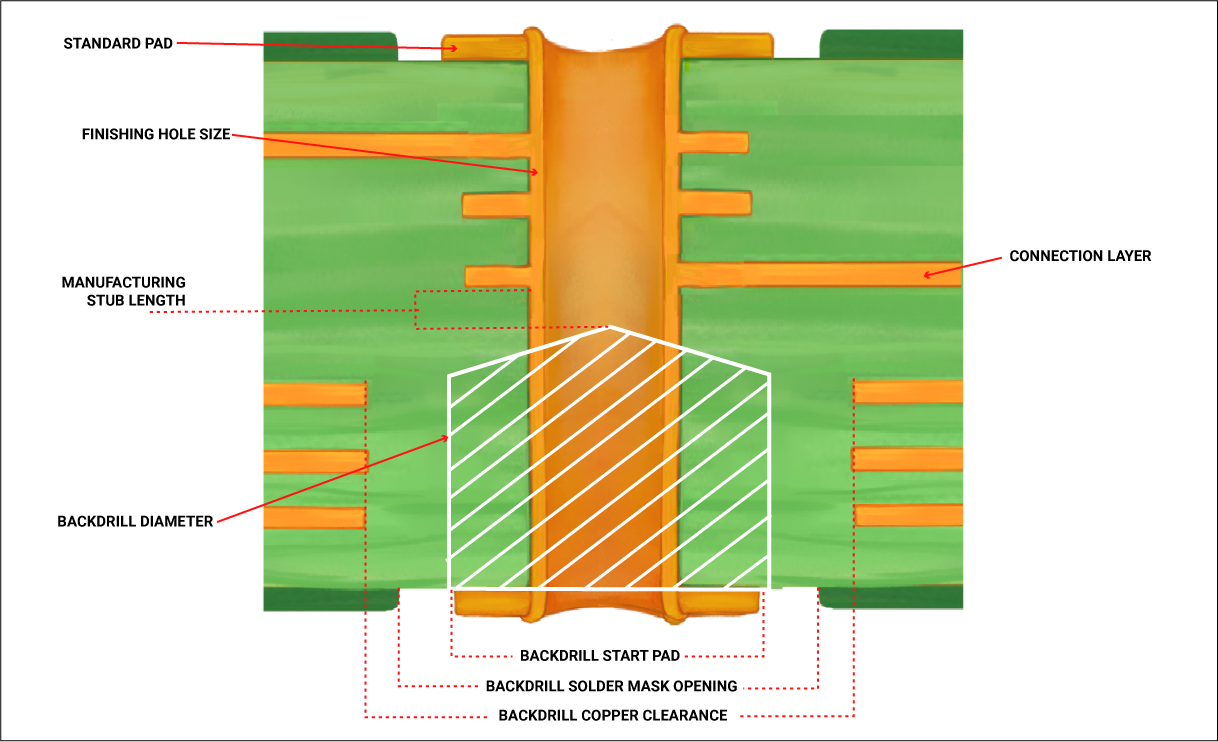
Back drilling in PCB involves drilling a hole slightly larger in diameter than the PTH to remove the conductive via stub.| Sierra Circuits
