Making Sense of Wave Soldering | Sierra Circuits
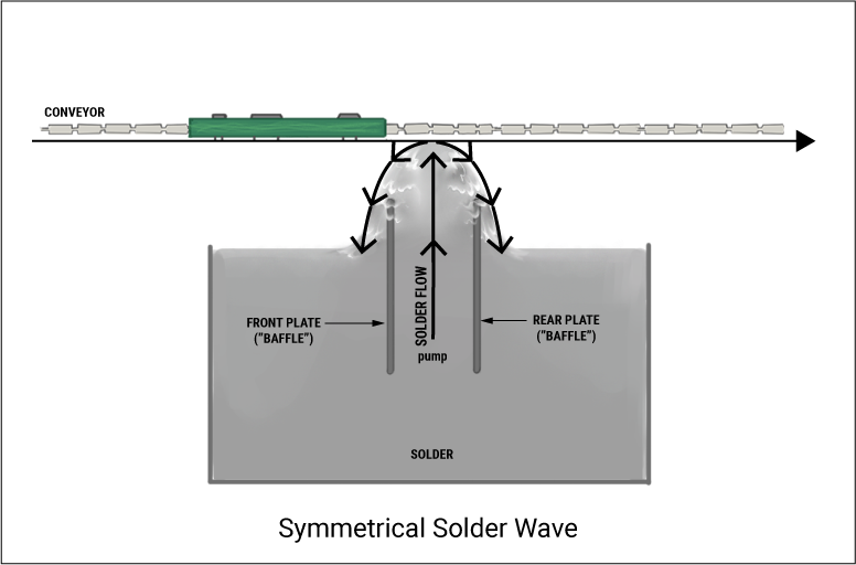
Wave soldering was the first practical automated mass soldering method for quickly soldering large numbers of components onto PCBs.| Sierra Circuits
Wave soldering was the first practical automated mass soldering method for quickly soldering large numbers of components onto PCBs.| Sierra Circuits
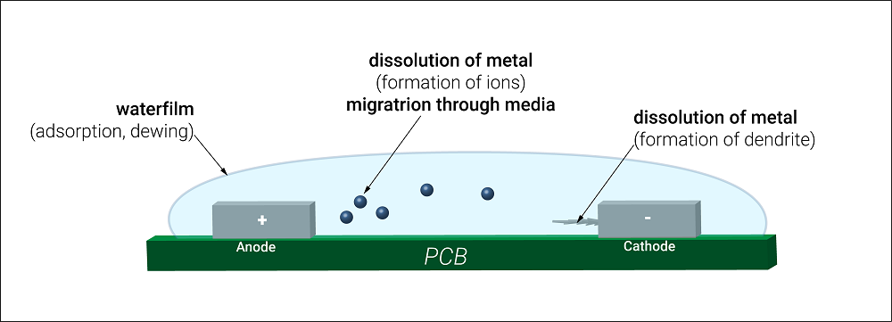
Did you know that more than 25% of PCB failures occur due to ionic contamination? Learn how to avoid issues with your board.| Sierra Circuits
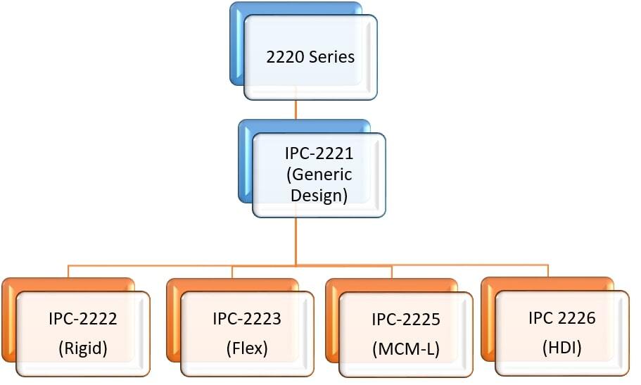
IPC-2221 is a standard that lays down the requirements for material selection, component placement, and high-voltage spacing requirements.| Sierra Circuits
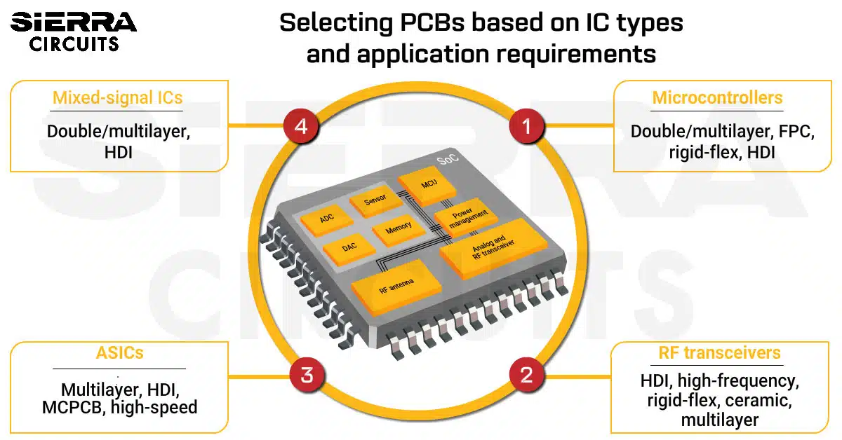
Selecting the right PCBs for IC integration depends on the chip’s signal characteristics, power demands, and the end-product.| Sierra Circuits
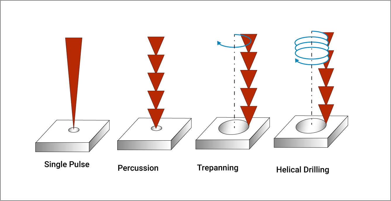
Laser drilling is performed to drill holes and vias on a PCB using a laser beam without compromising the board integrity.| Sierra Circuits
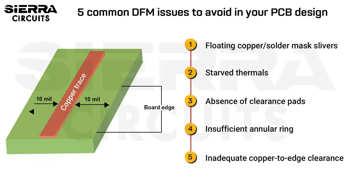
DFM checks each design before going for fabrication. It predicts potential defects and ensures board manufacturing with exact specifications.| Sierra Circuits
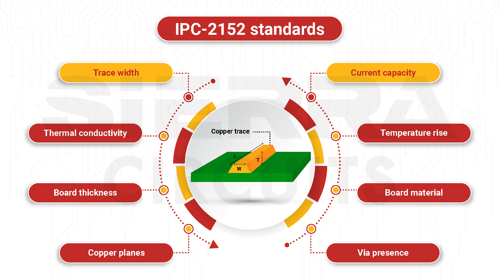
The IPC-2152 standard helps you optimize the current capacity, temperature rise, and width of a trace for efficient thermal management.| Sierra Circuits
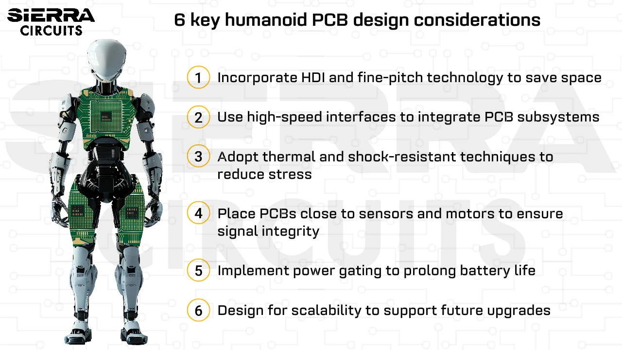
When designing humanoid robotics PCBs, use high-frequency materials and incorporate FPCs to integrate sensors.| Sierra Circuits
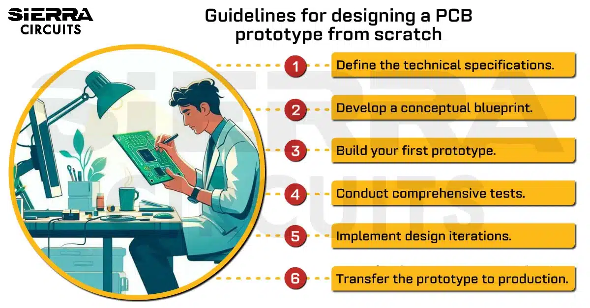
Designing a PCB prototype involves defining specifications, developing the system, testing, iterating, and validating with EVT samples.| Sierra Circuits
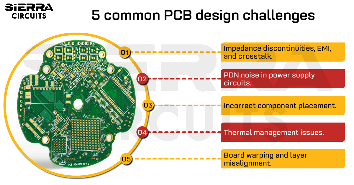
Learn the solutions for 5 common PCB design challenges like impedance discontinuities, EMI, crosstalk, part overlap, and PDN noise.| Sierra Circuits
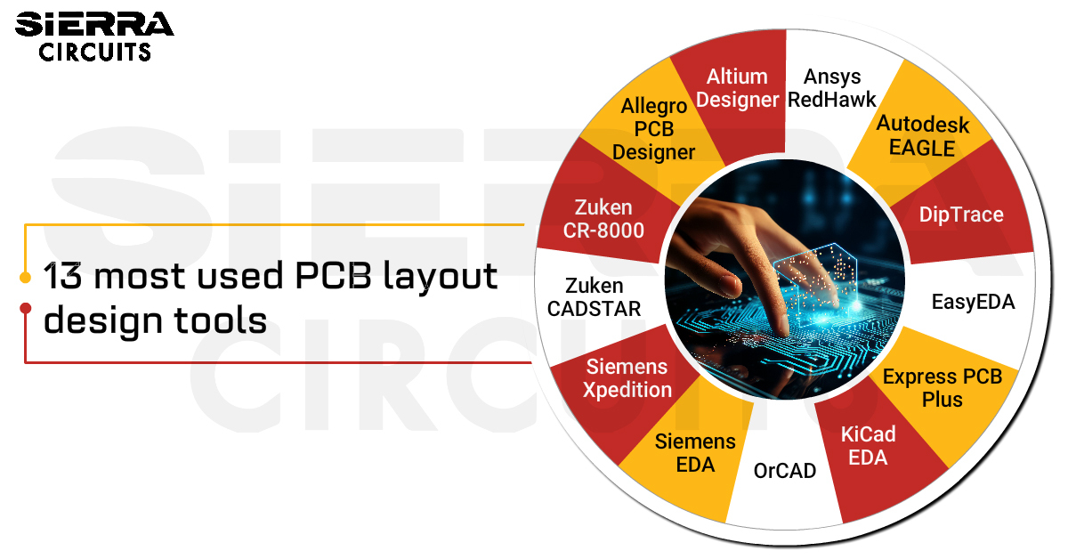
Some of the most used PCB layout design tools are Altium, Allegro, and KiCad. Consider UI, routing, and simulation before selecting one.| Sierra Circuits
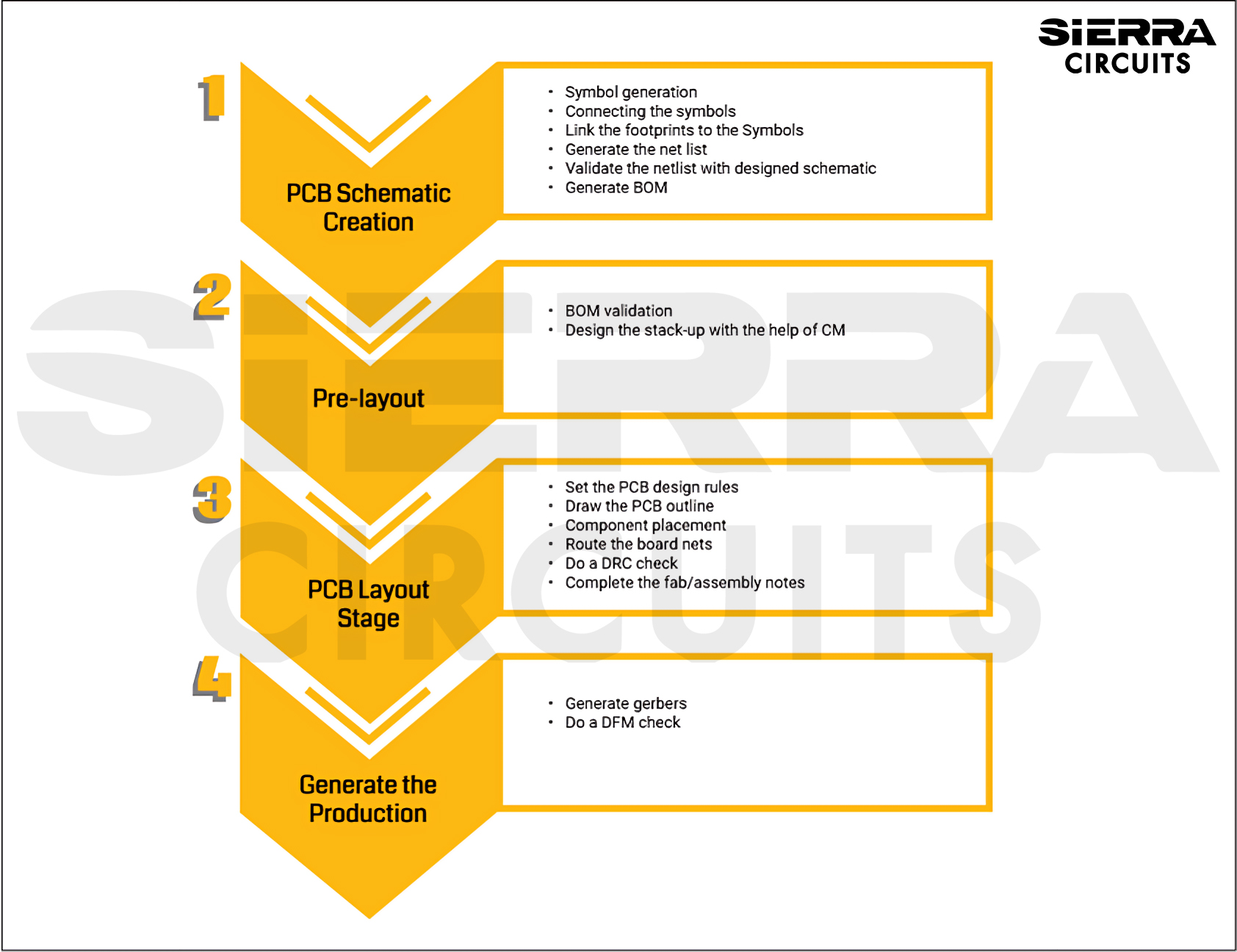
The PCB layout stage includes setting up the design tool, board outline, import of netlist, component placement, routing, silkscreen cleanup, and DRC check.| Sierra Circuits
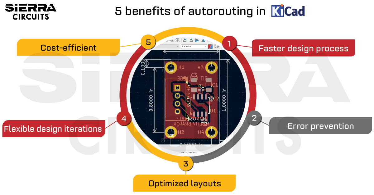
The autorouting plugin in KiCad automates the PCB routing process by creating optimized signal paths, improving the quality of your layouts.| Sierra Circuits
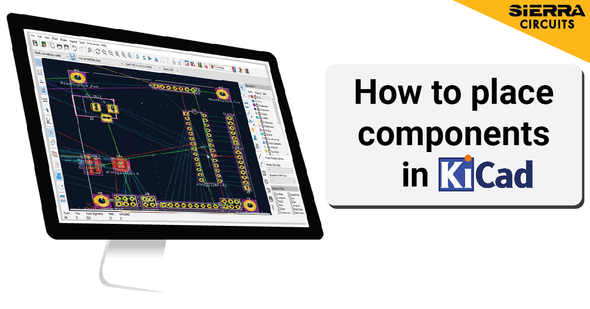
In this KiCad tutorial, you'll learn how to place components on your PCB layout and define your board outline.| Sierra Circuits
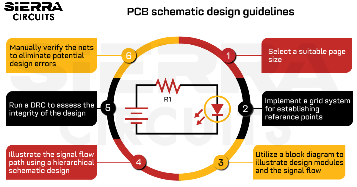
A PCB schematic must follow standard guidelines such as precision net labeling, and symbol standardization to have a well-structured design.| Sierra Circuits
