OhmegaPly and TCR with Embedded Passives | Sierra Circuits
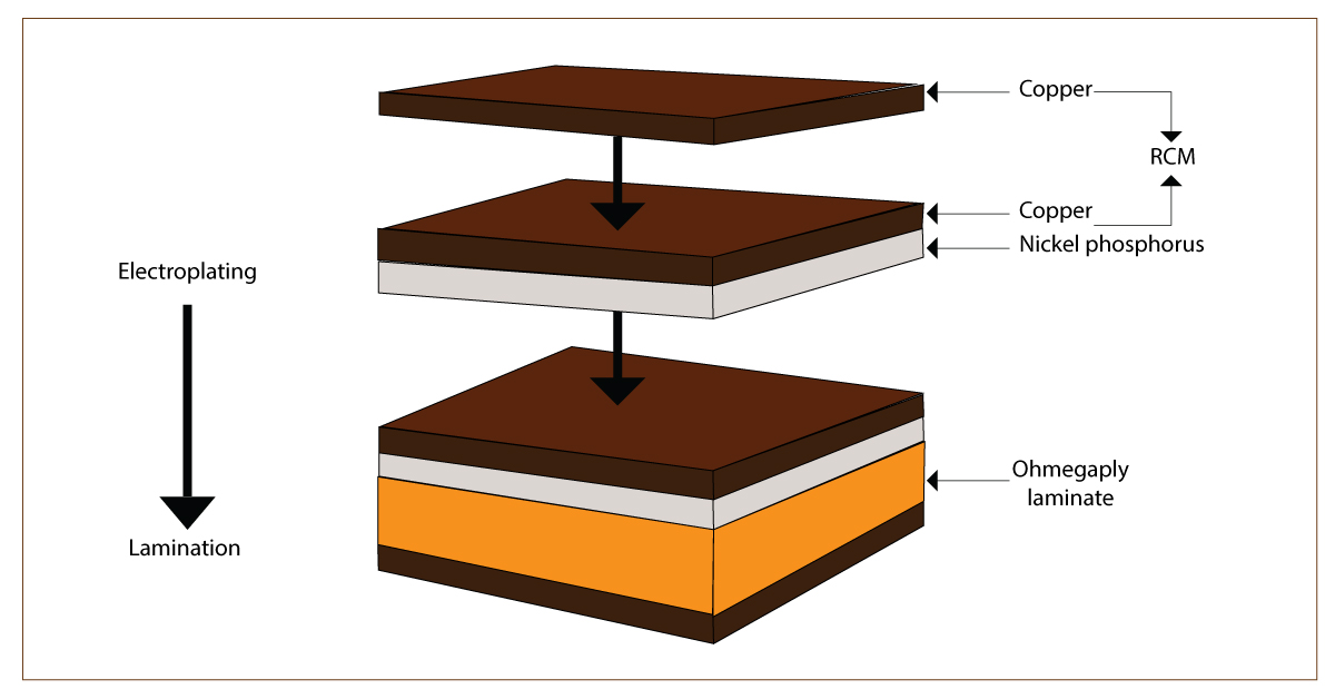
OhmegaPly and TCR follow the embedded passives technology that manufactures components like resistors and capacitors into the PCB substrate.| Sierra Circuits
OhmegaPly and TCR follow the embedded passives technology that manufactures components like resistors and capacitors into the PCB substrate.| Sierra Circuits
PCB layer count estimation is a critical step to achieving design success as it directly impacts the functional capability of your board.| Sierra Circuits
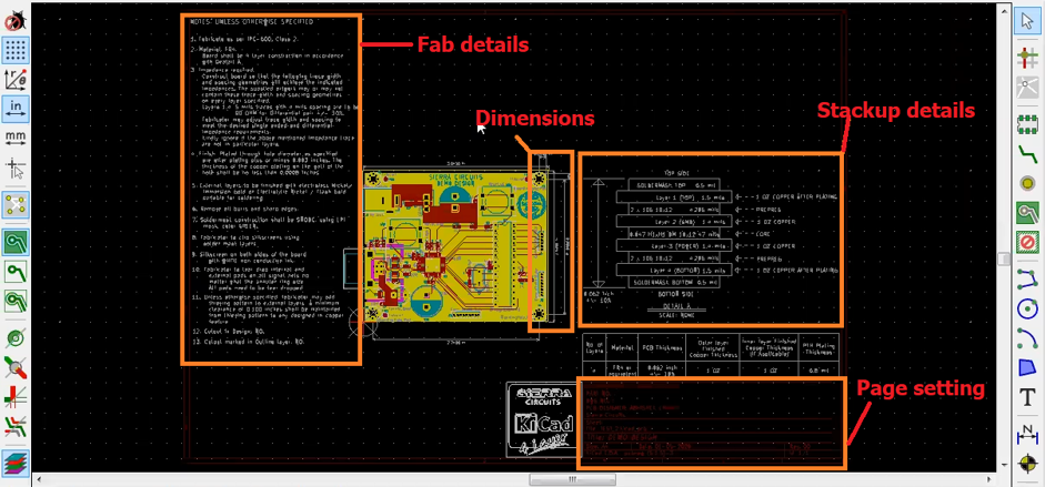
A PCB fab drawing is a reference document for manufacturing and includes all the information like board outline, stack-up, drilled holes, etc.| Sierra Circuits
Computer-Aided Manufacturing for PCBs is the use of software and computer-controlled machinery to perform tasks like drilling and component insertion.| Sierra Circuits
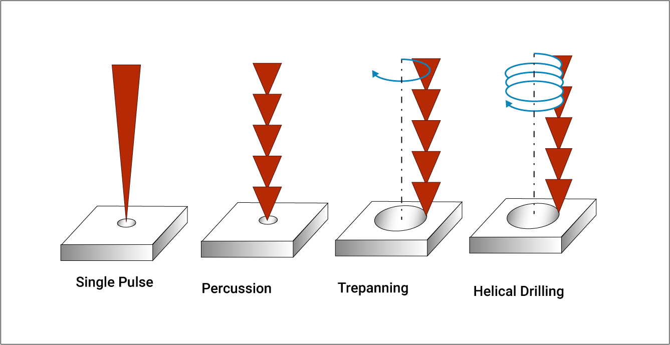
Laser drilling is performed to drill holes and vias on a PCB using a laser beam without compromising the board integrity.| Sierra Circuits
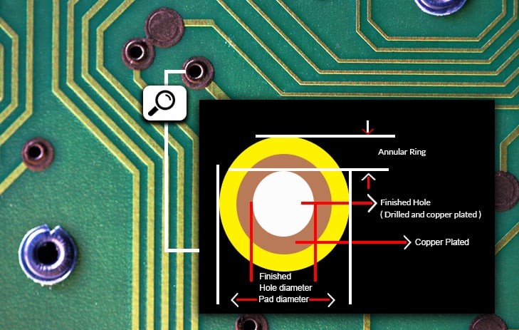
An annular ring is the copper area surrounding a plated via on a PCB. It establishes a solid connection between the via and copper traces.| Sierra Circuits
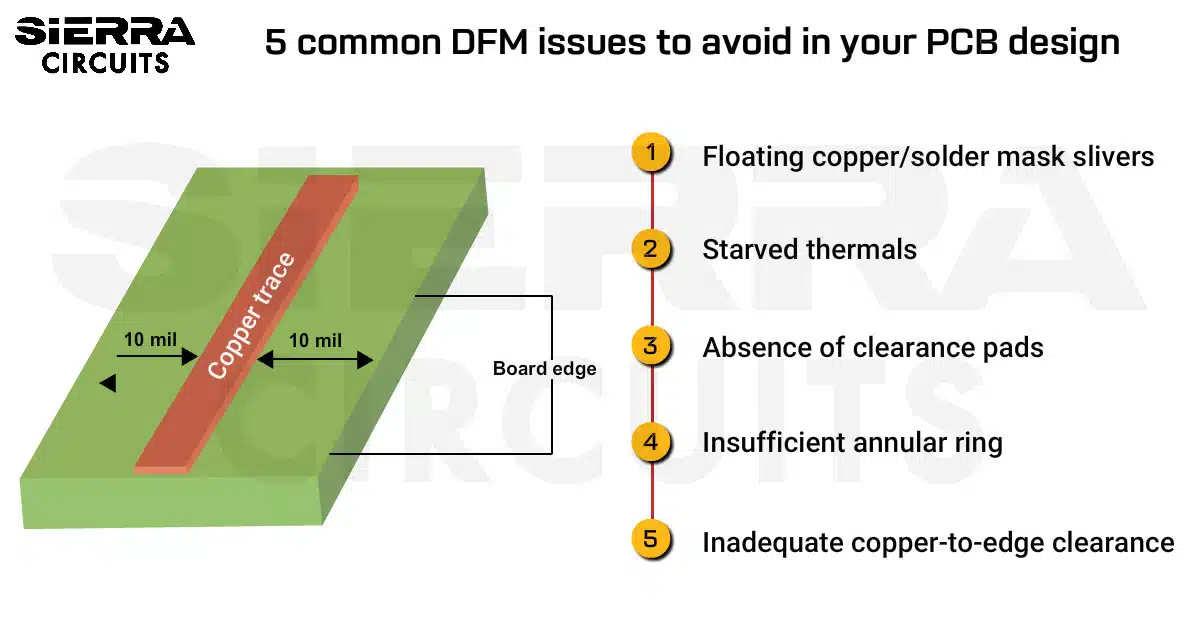
DFM checks each design before going for fabrication. It predicts potential defects and ensures board manufacturing with exact specifications.| Sierra Circuits
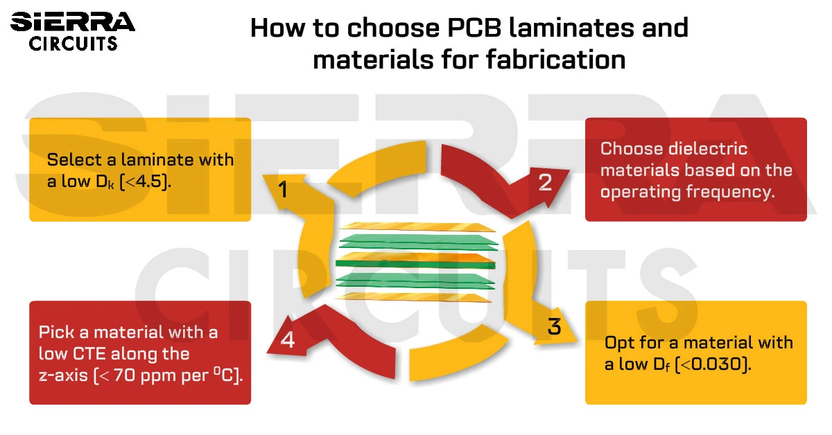
Selecting the right PCB laminates and materials for your design is very important as it can impact the overall performance of the board.| Sierra Circuits
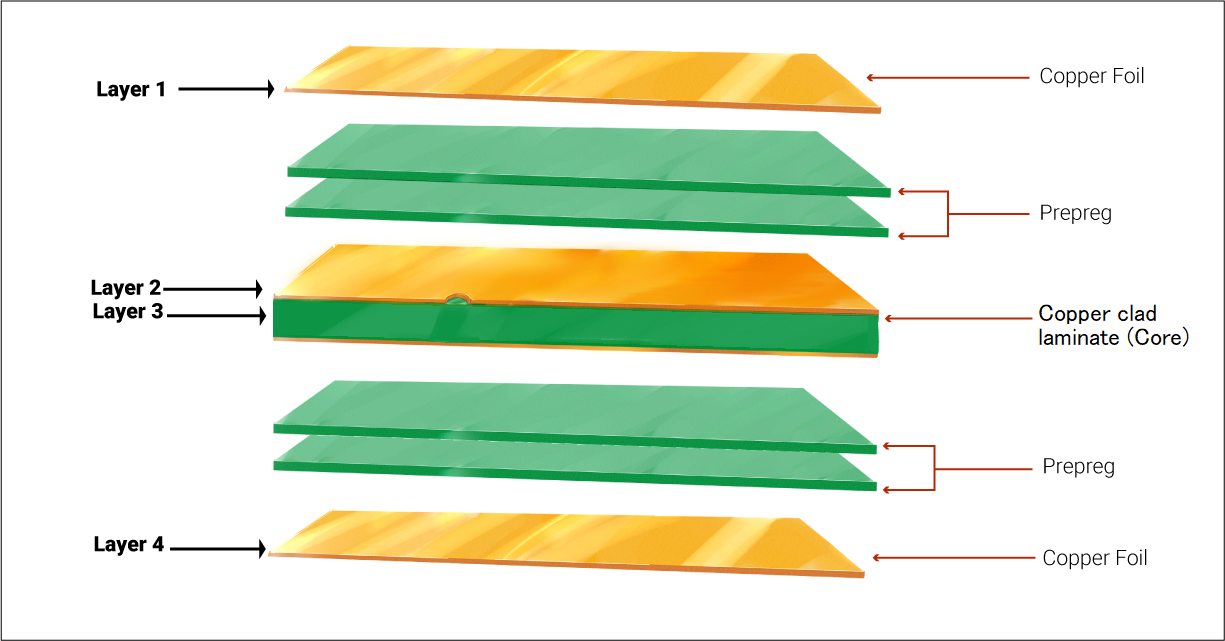
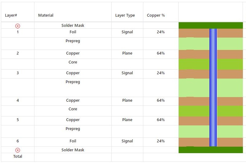
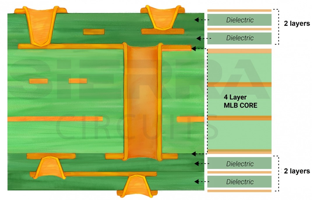
A multilayer PCB has more than two layers in its stack-up. The stack-up describes the construction of a multilayer board in sequential order.| Sierra Circuits
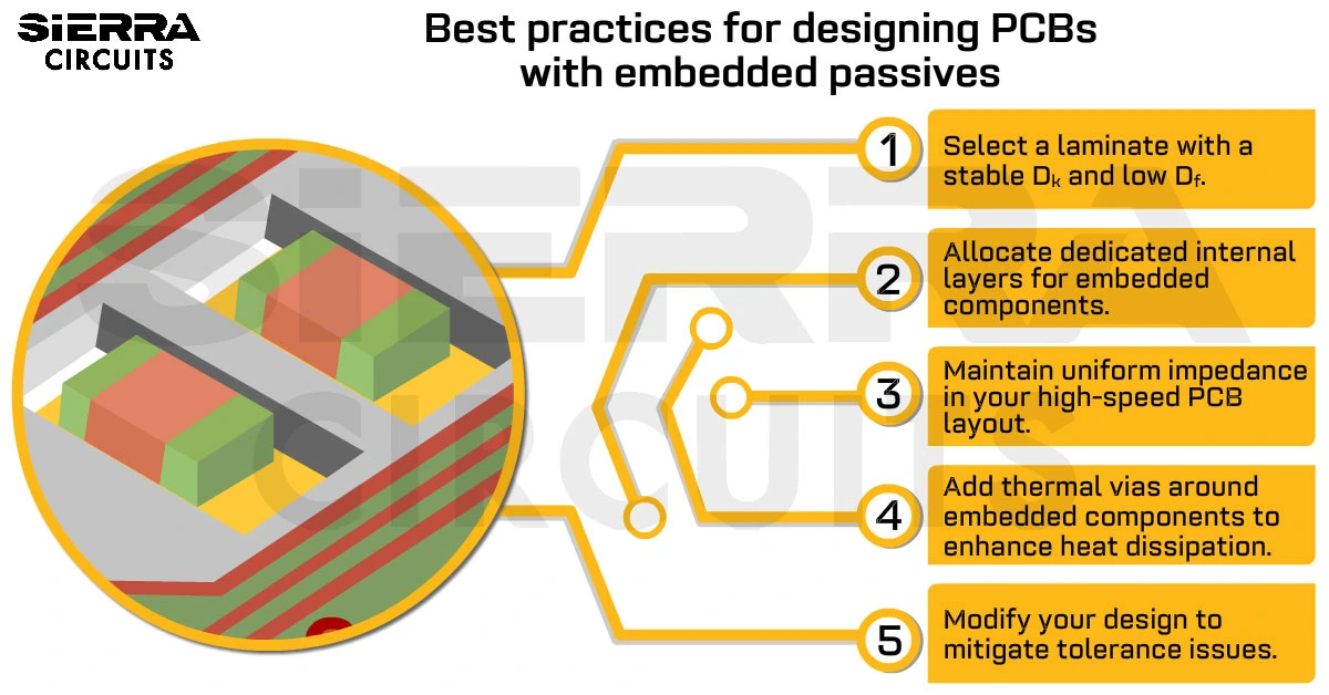
Embedded PCB components are passive devices fabricated within the PCB substrate. They reduce parasitic effects and enhance heat dissipation.| Sierra Circuits
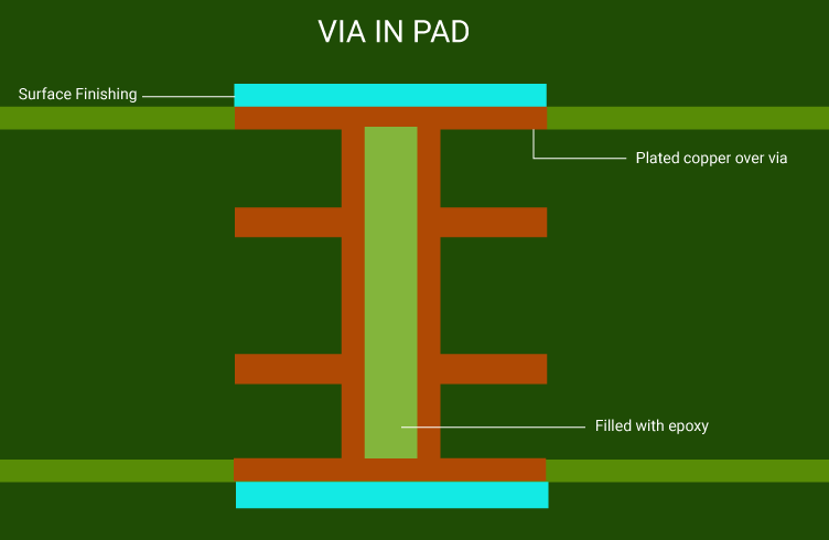
Use via-in-pad technology when the board size is limited, components have small footprints, and surface routing options are restricted.| Sierra Circuits
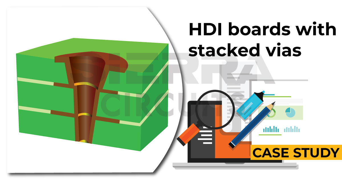
This case study focuses on the challenges and solutions that we implemented to design complex HDI boards with stacked vias.| Sierra Circuits
Vias are miniature conductive pathways drilled into the PCB to establish electrical connectivity between the different layers.| Sierra Circuits
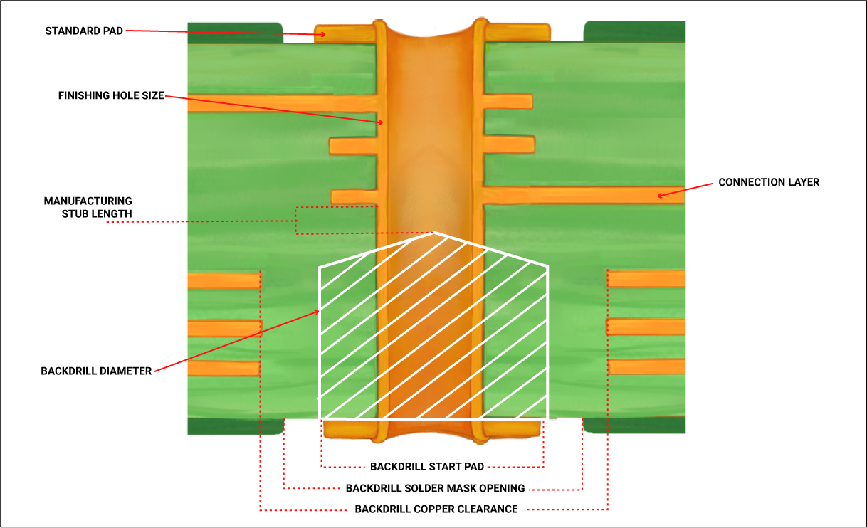
Back drilling in PCB involves drilling a hole slightly larger in diameter than the PTH to remove the conductive via stub.| Sierra Circuits
