
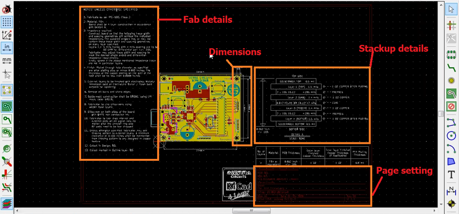
A PCB fab drawing is a reference document for manufacturing and includes all the information like board outline, stack-up, drilled holes, etc.| Sierra Circuits
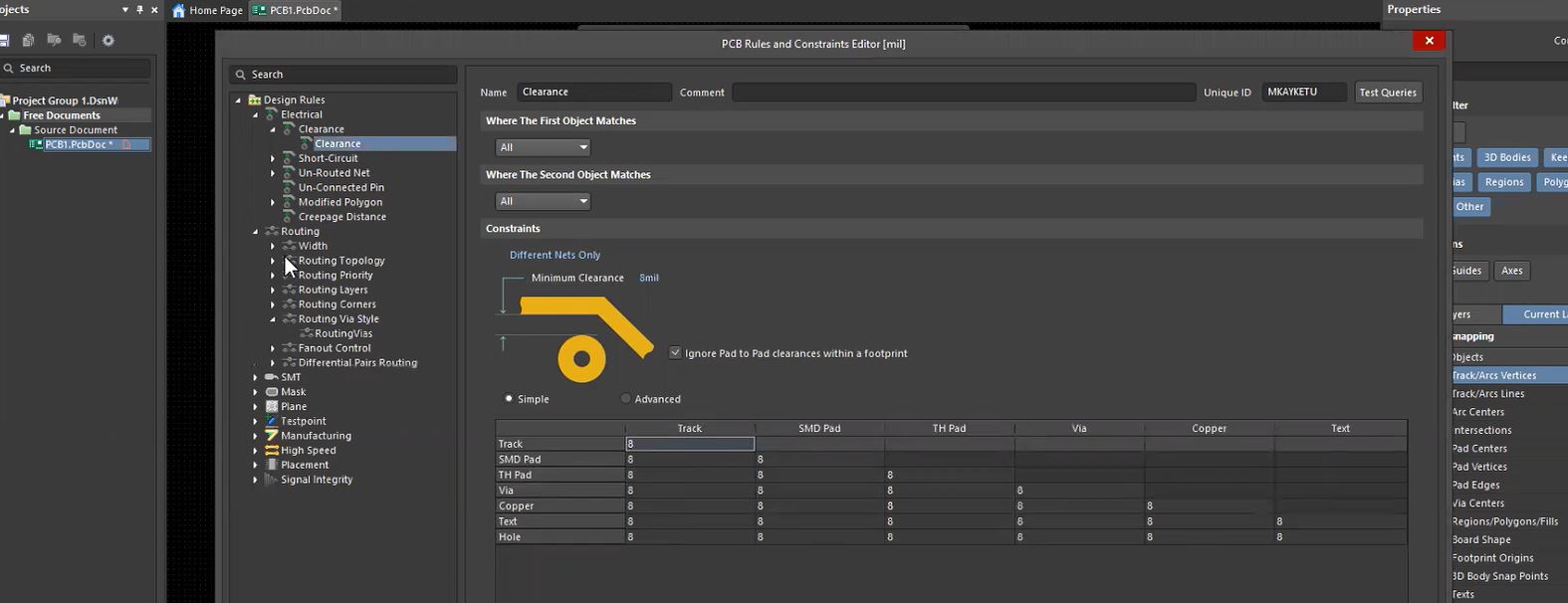
PCB constraint settings is crucial in board designing. Altium Designer and Allegro both come with attractive constraint management features.| Sierra Circuits
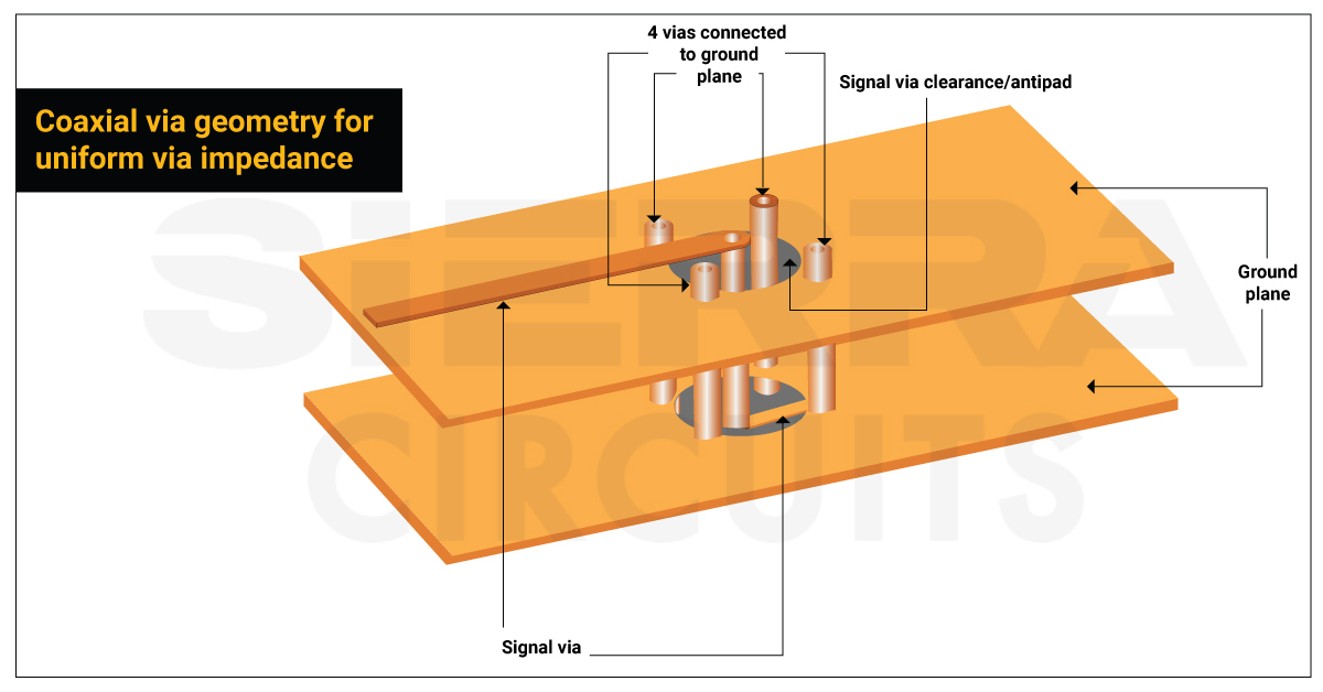
To achieve uniform via impedance, implement coaxial hole structures, and place ground via close to the signal via.| Sierra Circuits

To build an efficient PCB stack-up, select the right materials, estimate the number of signal layers, and optimally arrange the layers.| Sierra Circuits
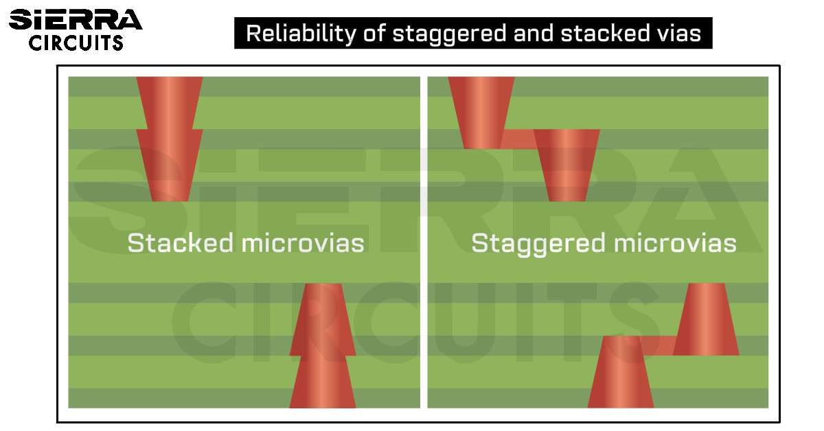
Staggered and stacked vias play crucial role in designing HDI boards. The compact design is highly functional with great signal integrity.| Sierra Circuits
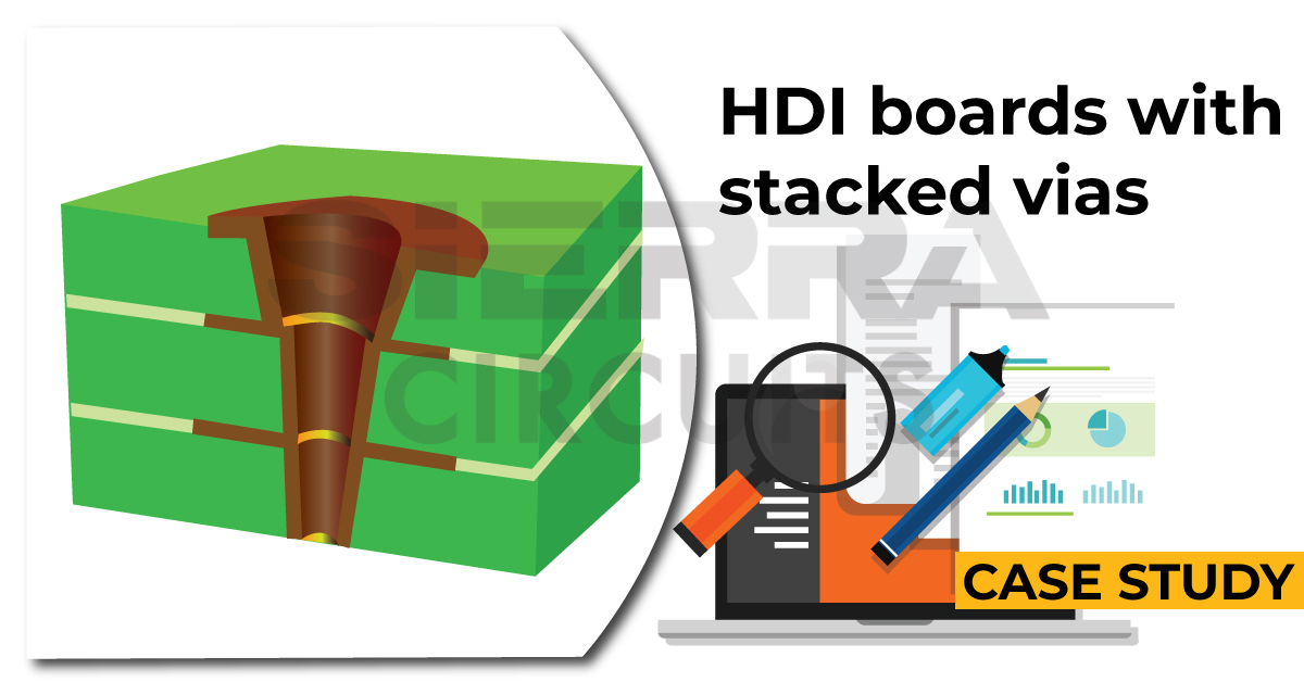
This case study focuses on the challenges and solutions that we implemented to design complex HDI boards with stacked vias.| Sierra Circuits