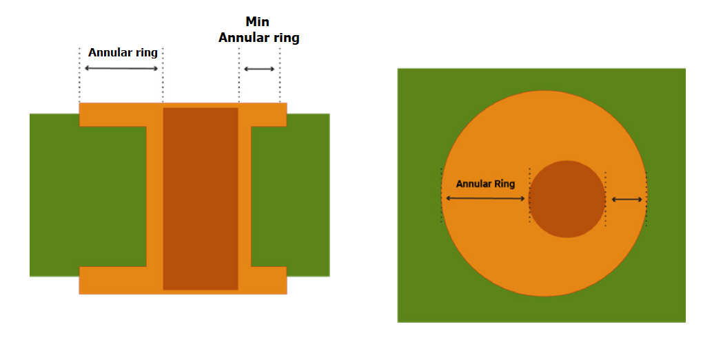
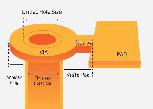
Annular Ring Size | Sierra Circuits
The minimum annular ring size should be greater than or equal to the values defined in the PCB design.| Sierra Circuits
The minimum annular ring size should be greater than or equal to the values defined in the PCB design.| Sierra Circuits
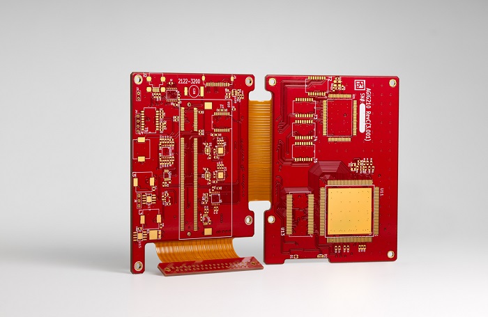
Rigid-flex PCB designs may be expensive to fabricate, but they can essentially save costs during electronic system assembly.| Sierra Circuits
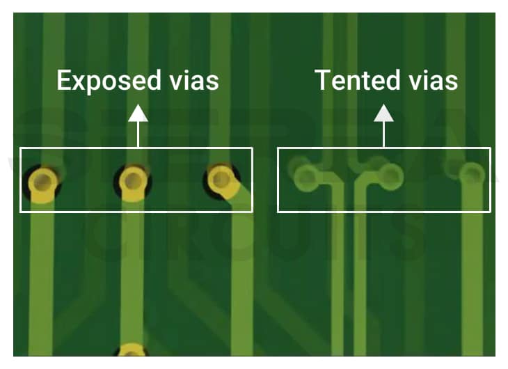
PCB via tenting protects vias from contamination, corrosion, and electrical shorts by covering exposed vias with a solder mask.| Sierra Circuits
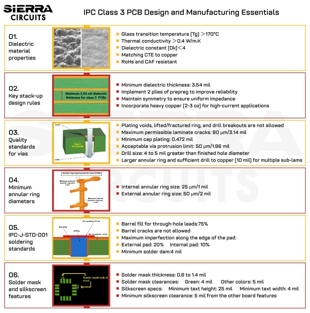
To build an efficient class 3 PCB, you need to design your stack-up, annular ring, and vias as per the IPC-6012 and IPC-A-610 standards.| Sierra Circuits
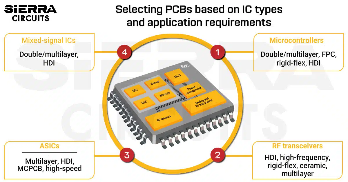
Selecting the right PCBs for IC integration depends on the chip’s signal characteristics, power demands, and the end-product.| Sierra Circuits
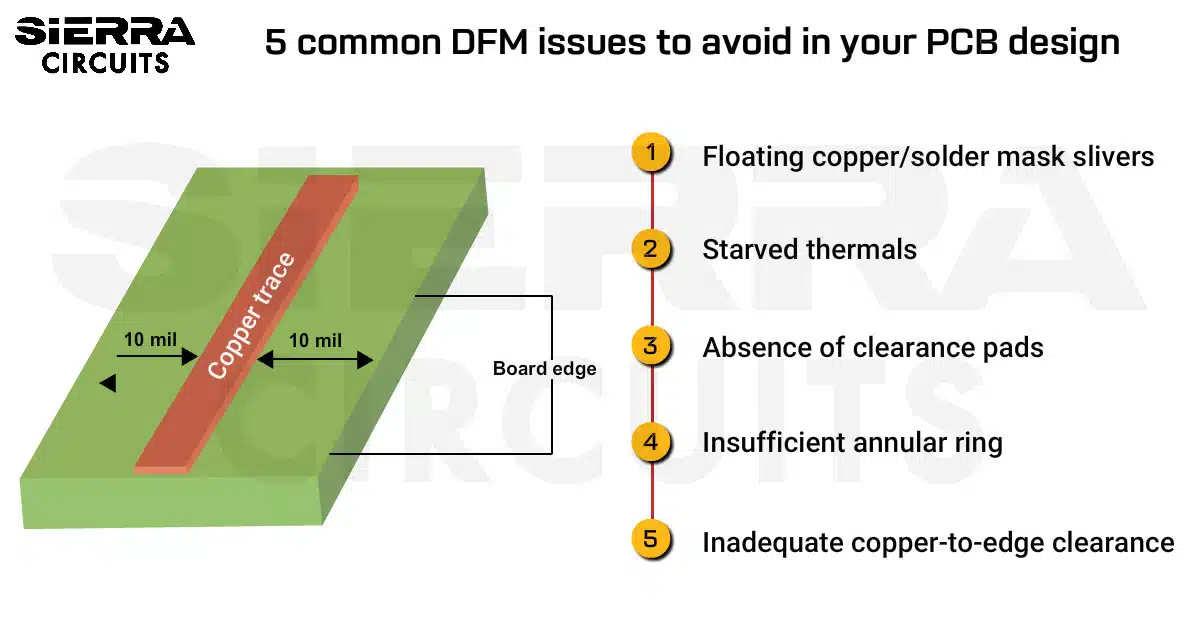
DFM checks each design before going for fabrication. It predicts potential defects and ensures board manufacturing with exact specifications.| Sierra Circuits
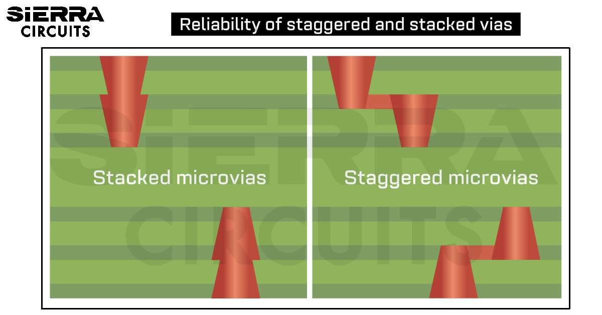
Staggered and stacked vias play crucial role in designing HDI boards. The compact design is highly functional with great signal integrity.| Sierra Circuits
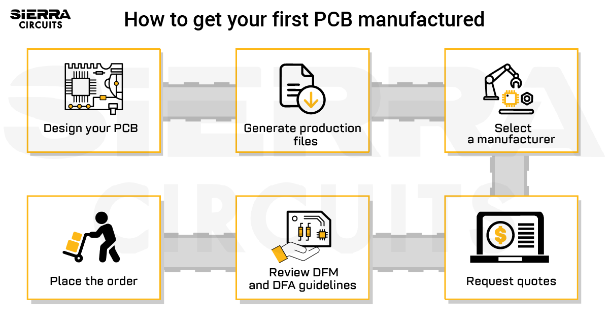
To get your first PCB manufactured, design your board, select a manufacturer, perform DFM and DFA analysis, and place the order.| Sierra Circuits
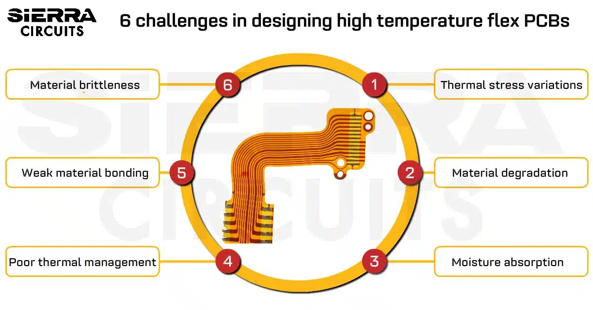
When designing high temperature flex PCBs, consider adhesiveless laminates, use cross-hatched ground planes, and incorporate stiffeners.| Sierra Circuits
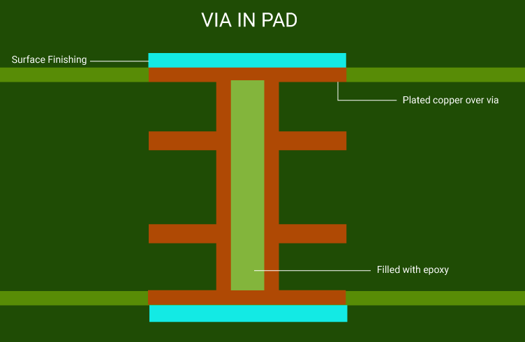
Use via-in-pad technology when the board size is limited, components have small footprints, and surface routing options are restricted.| Sierra Circuits
Drilling is the most expensive and time-consuming process in PCB manufacturing. A small fault in the drilling process leads to a great loss.| Sierra Circuits
