How to Choose the Right PCBs for IC Integration | Sierra Circuits
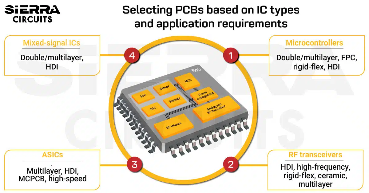
Selecting the right PCBs for IC integration depends on the chip’s signal characteristics, power demands, and the end-product.| Sierra Circuits
Selecting the right PCBs for IC integration depends on the chip’s signal characteristics, power demands, and the end-product.| Sierra Circuits
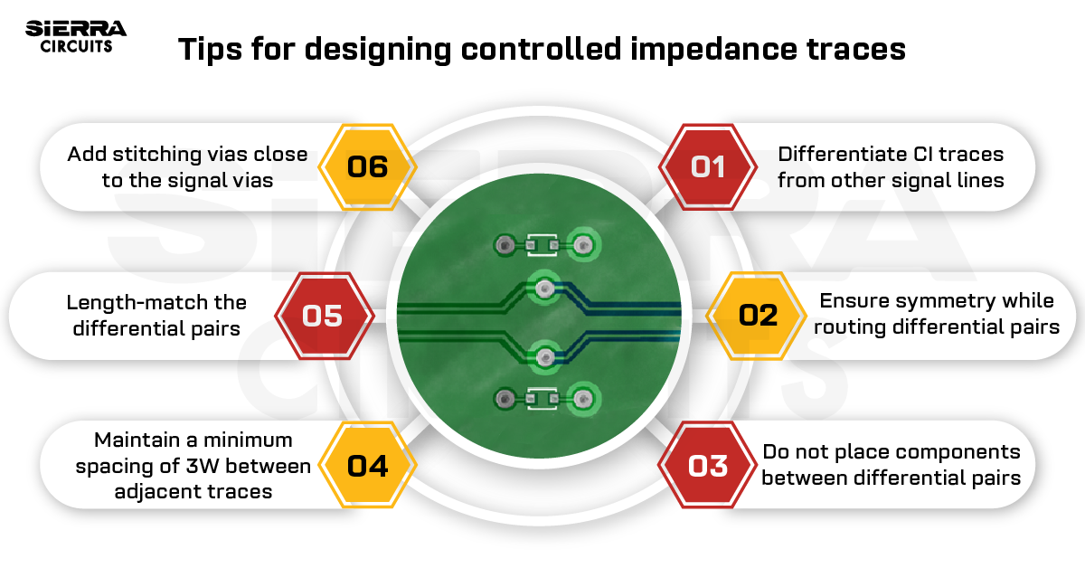
PCB materials, dielectric constant, trace height, and width affect the controlled impedance of a transmission line.| Sierra Circuits
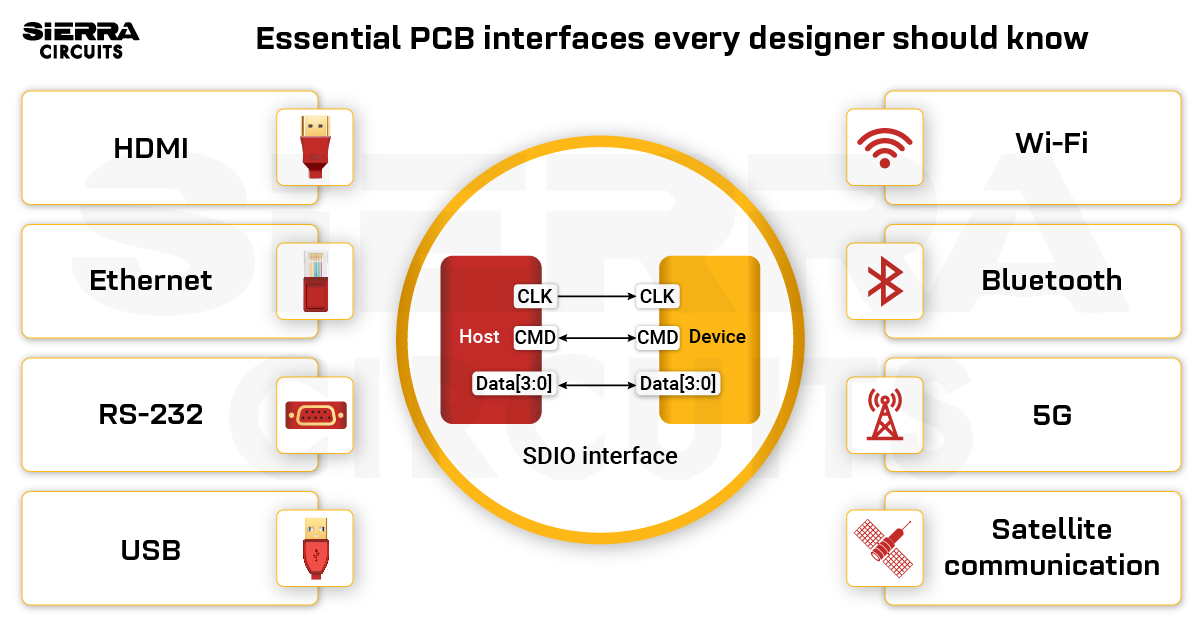
PCB interfaces are categorized into wired interfaces, like UART, I2C, and PCIe, and wireless interfaces, such as 5G, Wi-Fi, and LoRa.| Sierra Circuits
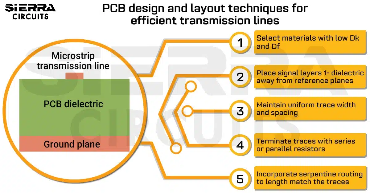
When designing PCB transmission lines, terminate the traces accurately and maintain a uniform trace width and spacing.| Sierra Circuits
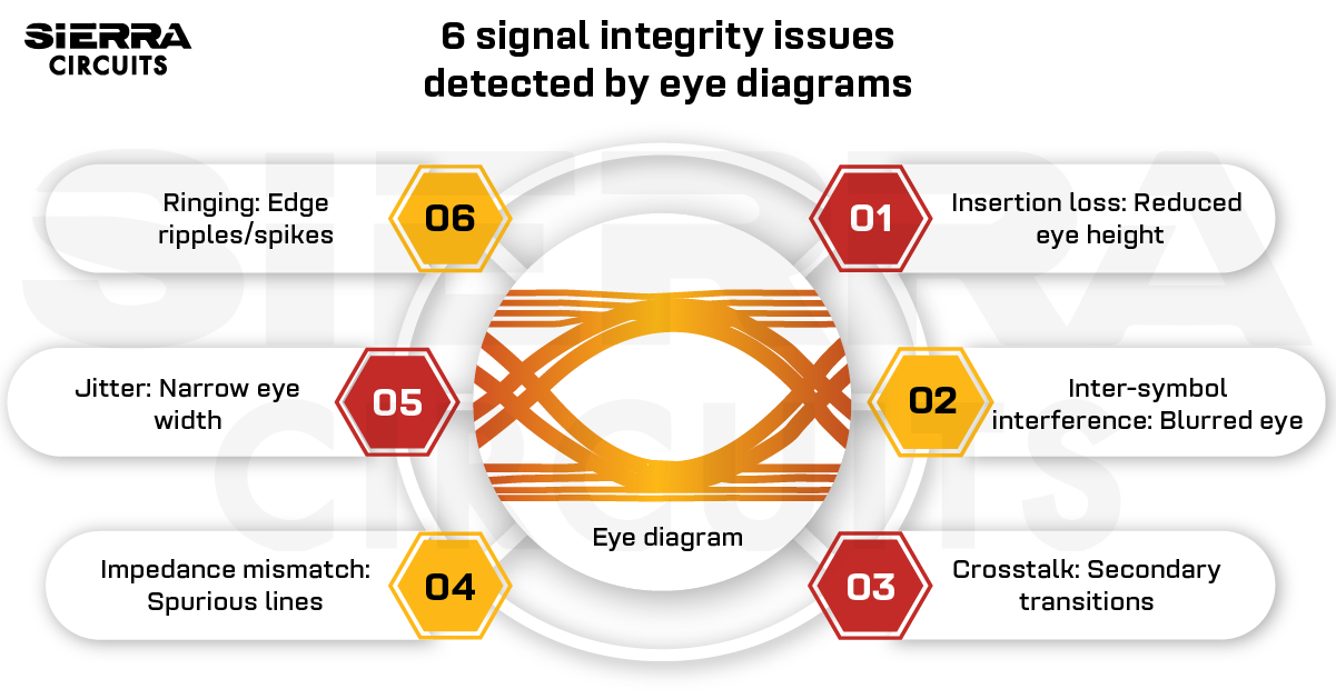
Eye diagrams reveal critical signal integrity issues like Inter-symbol interference, jitter, crosstalk, ringing, and reflections.| Sierra Circuits
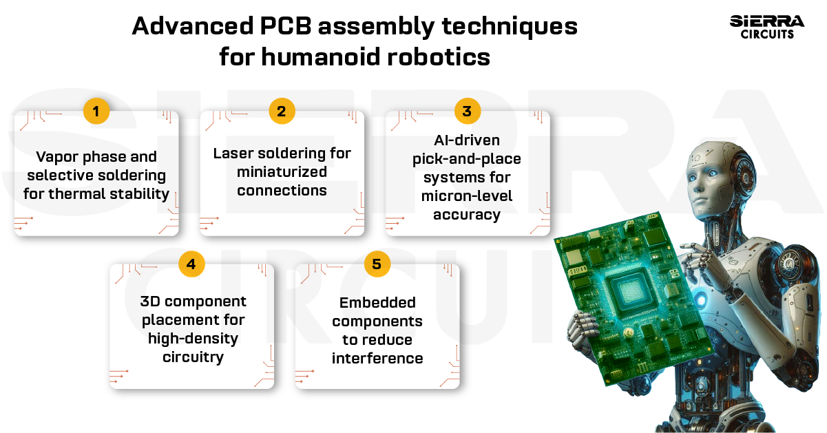
Humanoid robotics PCB assembly requires advanced techniques like AI-driven component placement and 3D circuit integration.| Sierra Circuits
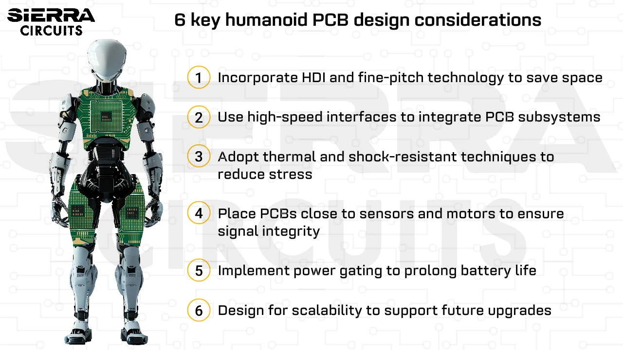
When designing humanoid robotics PCBs, use high-frequency materials and incorporate FPCs to integrate sensors.| Sierra Circuits

To avoid jitter in PCBs, terminate the traces efficiently and incorporate decoupling capacitors near clock drivers and receivers.| Sierra Circuits
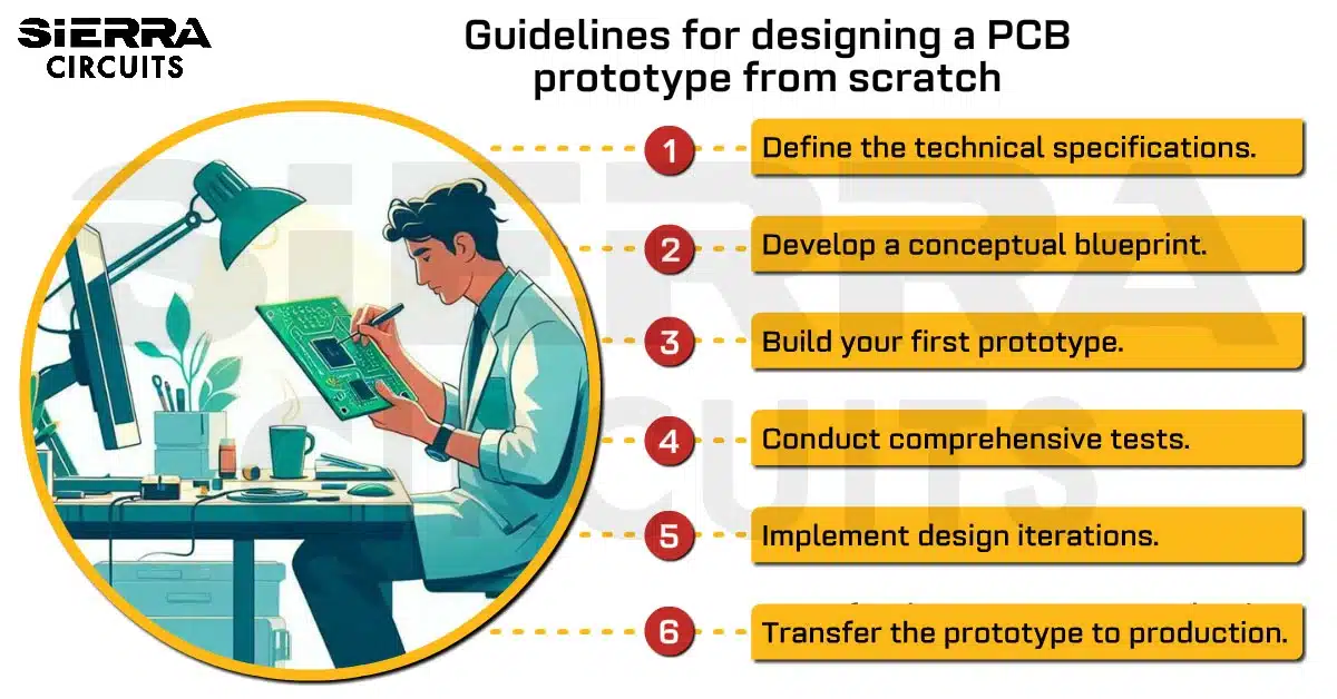
Designing a PCB prototype involves defining specifications, developing the system, testing, iterating, and validating with EVT samples.| Sierra Circuits
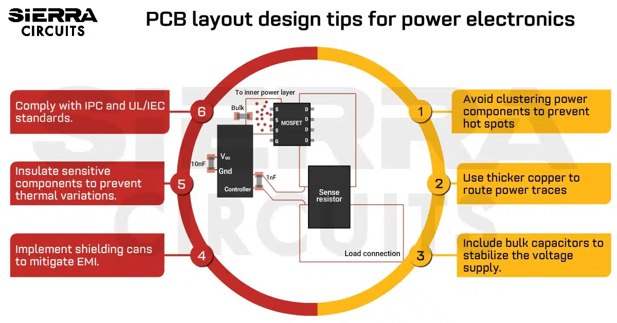
When designing a power electronics PCB, pick high thermal conductivity materials, integrate protection devices, and adhere to IPC standards.| Sierra Circuits
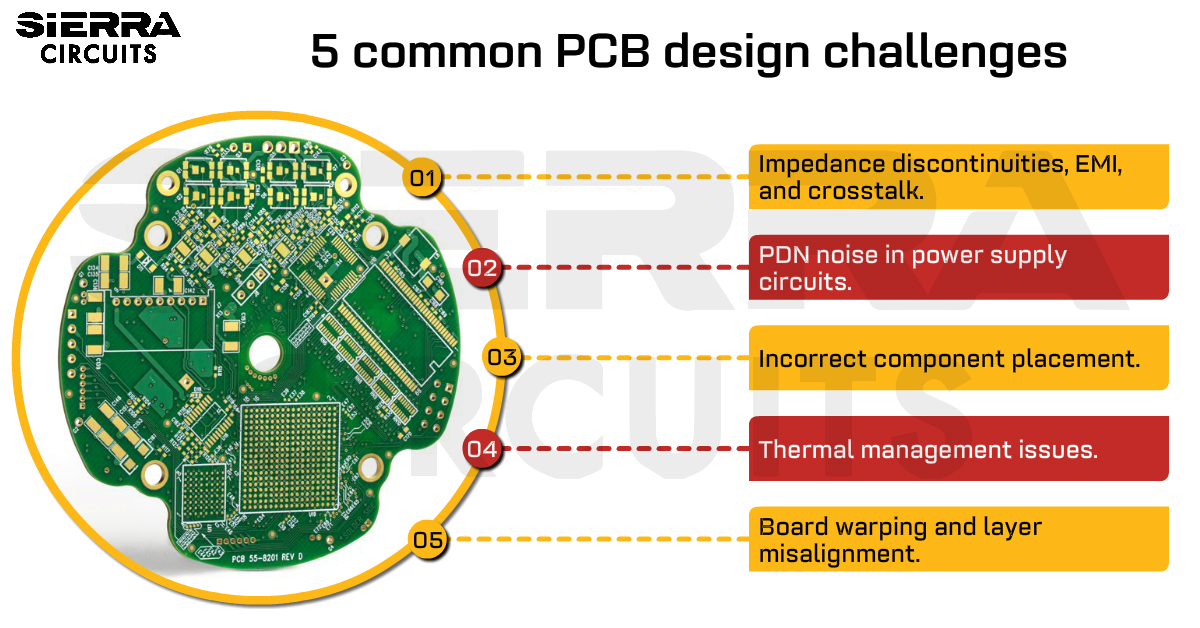
Learn the solutions for 5 common PCB design challenges like impedance discontinuities, EMI, crosstalk, part overlap, and PDN noise.| Sierra Circuits
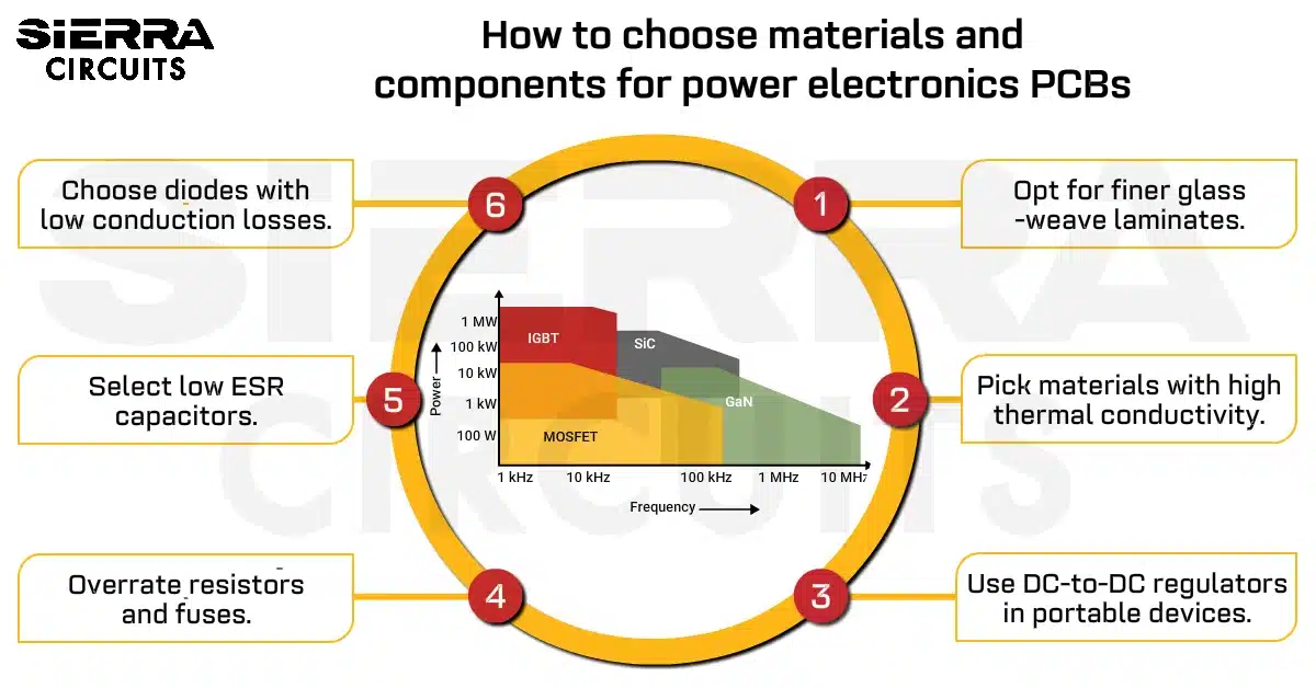
Effective component selection for power electronics PCBs focuses on low-loss diodes, low ESR capacitors, and low DCR inductors.| Sierra Circuits
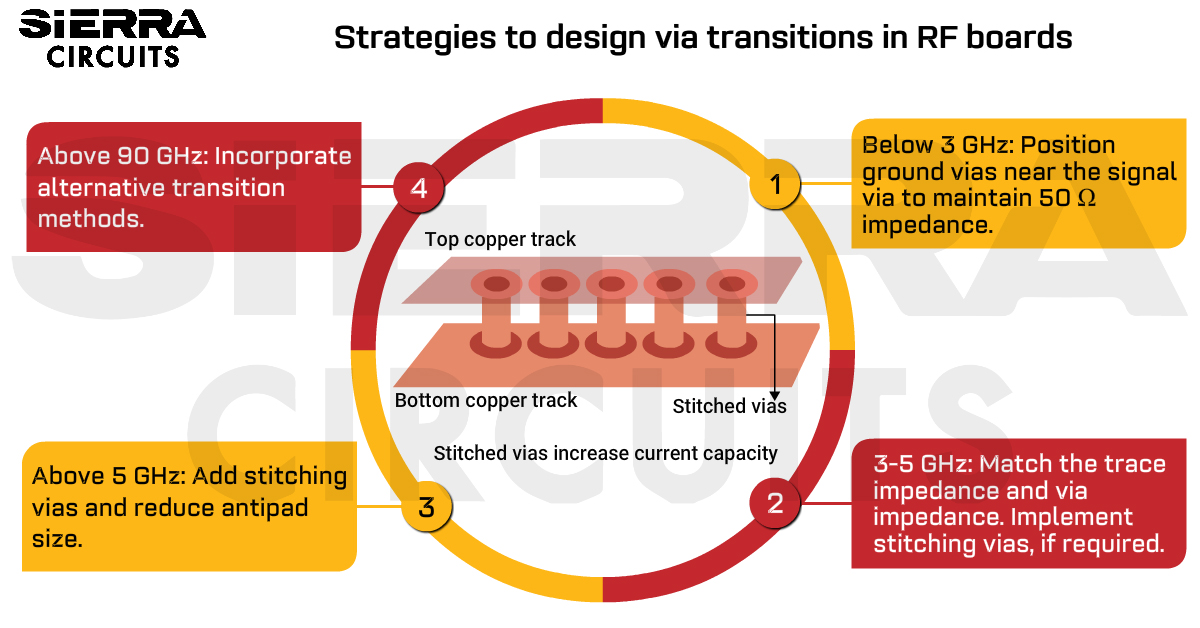
When designing RF PCB vias, ensure uniform impedance and consider parasitic effects, controlled impedance, and ground via placement.| Sierra Circuits
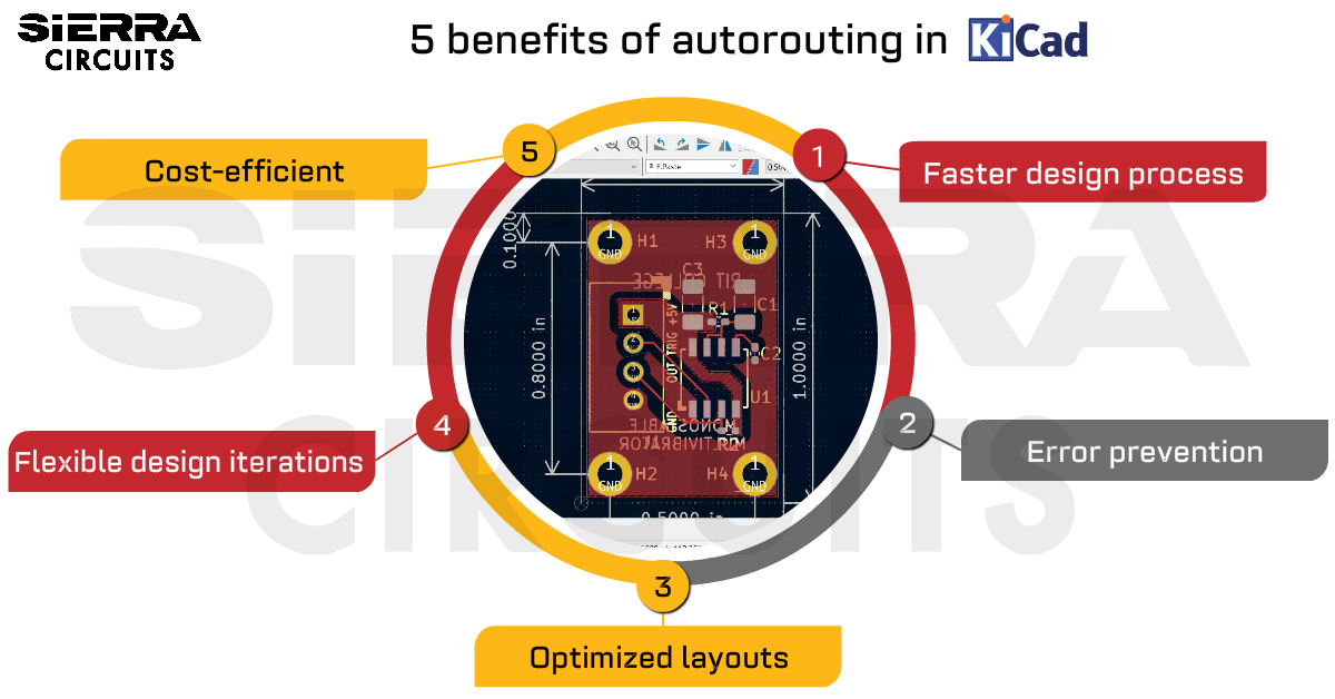
The autorouting plugin in KiCad automates the PCB routing process by creating optimized signal paths, improving the quality of your layouts.| Sierra Circuits
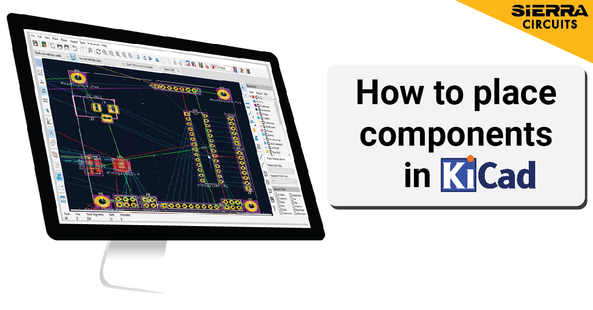
In this KiCad tutorial, you'll learn how to place components on your PCB layout and define your board outline.| Sierra Circuits
To design a microwave PCB, select materials with low dielectric constant, prefer CPWs, and add board-level shielding to mitigate EMI effects.| Sierra Circuits
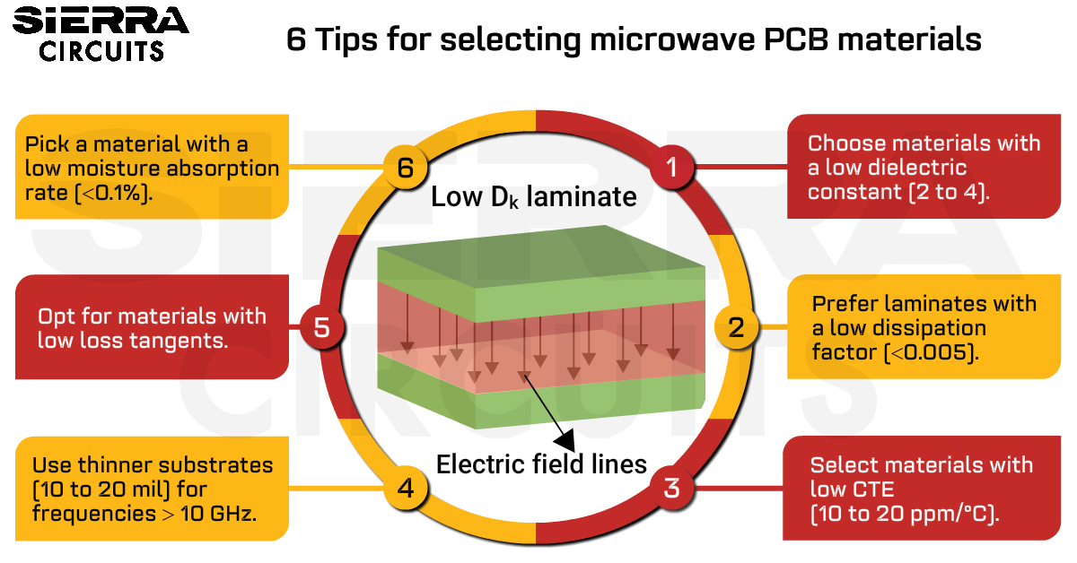
To design a microwave PCB, select materials with low dielectric constant, dissipation factor, and CTE and prefer CPW transmission lines.| Sierra Circuits
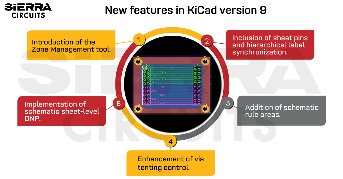
KiCad version 9 is set to add features like the new zone manager, sheet pin and label synchronization, and schematic sheet-level DNP.| Sierra Circuits
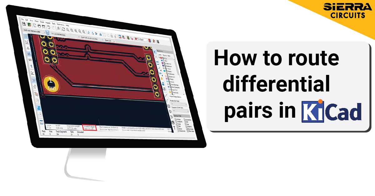
In this KiCad tutorial, you'll learn how to route differential pairs, fine-tune lengths, and manage skew to ensure signal integrity.| Sierra Circuits
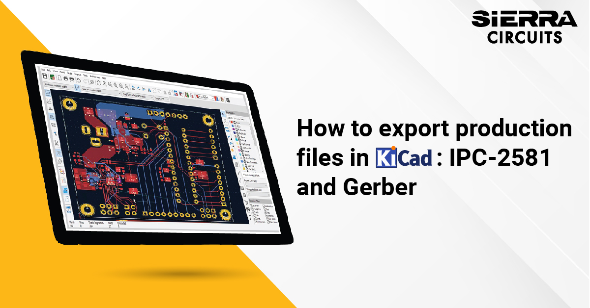
In this KiCad tutorial, you will learn how to export IPC-2581, Gerber, and other production files such as drill files, netlist and BOM.| Sierra Circuits
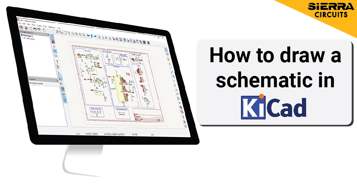
In this KiCad tutorial, you will learn how to create a schematic and build a custom symbol library from scratch.| Sierra Circuits

Modular PCB design breaks down complicated networks into small functional units, allowing you to keep track of your design and avoid errors.| Sierra Circuits
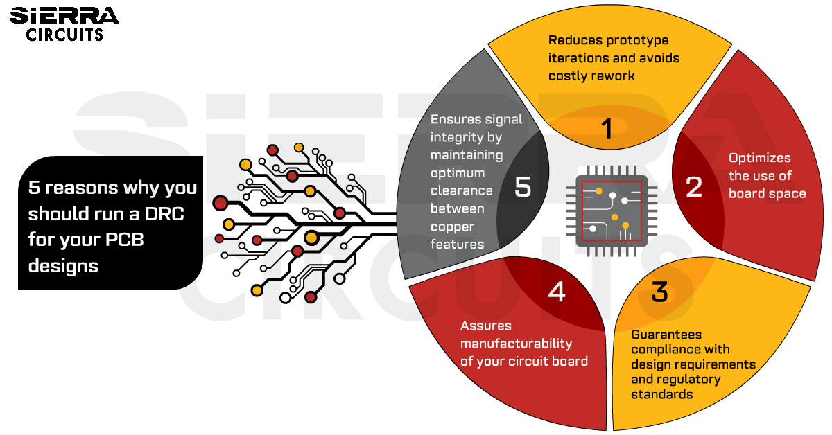
DRC helps you validate whether your PCB layout conforms to predefined constraints such as trace width, clearances, and hole sizes.| Sierra Circuits
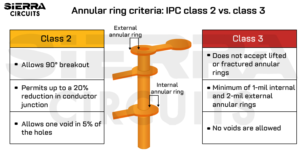
This article will help you understand the different PCB design rules for IPC Class 2 and Class 3 printed circuit boards.| Sierra Circuits
