
Profile - will - SierraConnect
Review the terms of service for the SierraConnect PCB forum. Learn about user responsibilities, privacy policies, and the legal guidelines for using our platform.| SierraConnect
Review the terms of service for the SierraConnect PCB forum. Learn about user responsibilities, privacy policies, and the legal guidelines for using our platform.| SierraConnect

Review the terms of service for the SierraConnect PCB forum. Learn about user responsibilities, privacy policies, and the legal guidelines for using our platform.| SierraConnect

Most of the time: Schematics and PCBs for systems with data paths up to 10Gbps, High-speed digital design, Analogue, PSUs, FPGAs, etc. Some of the time: Data links to 26Gbps, from multiple ADCs, via optical, Signal integrity, Power integrity. The rest of the time (the fun bits): Analysis of the Space-radiation environment, measuring the effects of high-energy particles on semiconductors.| SierraConnect

My name is Eduardo Mateos. I was born in Galapagar, a small town close to Madrid (SPAIN). I am Telecommunications Engineer (Universidad Politécnica de Madrid) and I have worked for more than 30 years in the microwave and high speed digital signals areas. At the moment I work by Avago Technologies, a Broadcom Inc Company, in Regensburg (Germany).| SierraConnect

Review the terms of service for the SierraConnect PCB forum. Learn about user responsibilities, privacy policies, and the legal guidelines for using our platform.| SierraConnect

Review the terms of service for the SierraConnect PCB forum. Learn about user responsibilities, privacy policies, and the legal guidelines for using our platform.| SierraConnect
What is the best practice for tenting vias? Is it only one side or both. I used to know that tenting should be done on only one side to allow outgassing and avoid trapped air during reflow. But I heard the opposite recommendation, where it says that vias should be either tented on both sides or there should be no tenting at all left, as single sided tenting can introduce other reliability concerns.| SierraConnect - Latest posts
Designing a PCB isn’t only about achieving reliability. It’s also about balancing costs and manufacturability. Factors such as material type, number of layers, board size, drilling, and surface finish impact the overall budget. In this infographic, we break down the key PCB cost drivers and a few decision-making tips that help you save money. Material type The PCB laminate forms the foundation of your circuit and has a major impact on both cost and performance. Standard FR-4 laminates are...| SierraConnect - Latest posts
I’m designing a 2-layer PCB where the top layer is densely packed with through-hole and surface-mount components, while the bottom layer has minimal routing. From an EMI/EMC perspective, which ground plane strategy would be theoretically optimal: Ground plane (copper pour) on the top layer only Ground plane (copper pour) on the bottom layer only Ground planes on both layers with stitching vias I believe option 2 might be superior since it provides low-impedance return paths and minim...| SierraConnect
Originally published at: https://www.protoexpress.com/blog/techniques-to-measure-and-avoid-jitter-in-pcbs/ A signal’s deflection from its ideal rising and falling edges is called a jitter in PCB. The jitter in clock signals can impact the timing synchronization and consequently disrupt the overall signal integrity of the system. Clock signals with less jitter are essential to meet high-speed data communication. Non-uniform impedance, crosstalk, interference, and power supply noise are some ...| SierraConnect
Originally published at: https://www.protoexpress.com/blog/why-choose-halogen-free-pcbs-for-sustainable-electronics/ Halogen-free PCB materials are eco-friendly dielectrics that eliminate hazardous toxins while meeting sustainability standards without compromising performance. Halogen-based laminates can release toxic fumes during combustion or disposal, but halogen-free alternatives significantly reduce health and environmental risks. If you’re a PCB designer, product engineer, compliance ...| SierraConnect - Latest posts
I’m designing a 4-layer PCB where the two inner layers are solid ground planes, and the outer layers carry signals. Since I’ve always added ground pours on 2-layer designs, I’m wondering should I still add ground pours with stitching vias on the outer layers when internal ground planes are already present?| SierraConnect - Latest posts
Hello everyone, I have a Gerber file set for a PCB that was designed around 7–8 years ago. Unfortunately, I don’t have the original PCB design source file (like Altium, Eagle, etc.), only the Gerbers. I need to generate the XY coordinates (Pick & Place file) for SMT machine assembly. Could anyone guide me on: Whether it’s possible to extract or reconstruct XY coordinates directly from Gerber files, Any tools or scripts (open-source or commercial) that can help generate component placeme...| SierraConnect - Latest posts
Have a PCB question? Ask below in this thread. Ask Us Anything about... PCBs 2025-10-15 13:00 (America/Los_Angeles) → 2025-10-15 17:00 (America/Los_Angeles)| SierraConnect - Latest posts
See the Q&A: QuestionAnswer When I transition to and from stripline to microstrip, I put gnd vias close to the transition. How important is it to stitch the ground planes together at other locations? Why?As you pointed out, the importance of stitching ground planes together depends largely on the frequency of operation. The farther away the stitching vias are from the transition, the less impact they have on the circuit’s performance. A useful way to think about this is in terms of waveleng...| SierraConnect - Latest posts
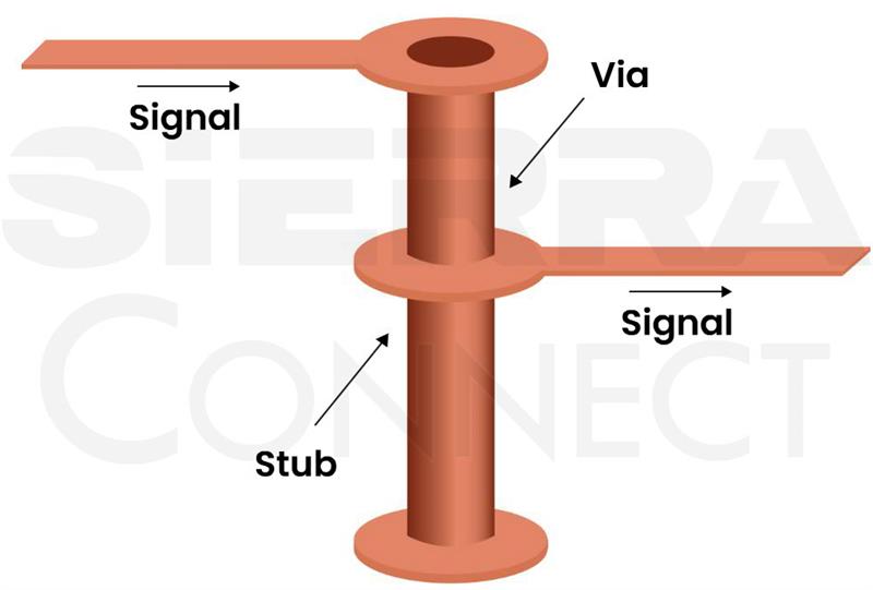
A via stub is the unused, plated portion of a via barrel that extends beyond the signal layers it is intended to connect. The unused segment behaves like an open-circuited transmission-line stub, introducing reflections, increased capacitance, and insertion loss. The reflections caused by the stub can interfere constructively or destructively with the main signal, leading to data errors or reduced eye opening. As a PCB designer, you should aim to eliminate via stubs to maintain signal integri...| SierraConnect
Hi everyone, I’m designing a PCB that will switch 230 VAC at about 8 A using a relay. I’m still learning and would like to check if my understanding is correct: Trace width: At 50 Hz (mains), skin effect is negligible, so I can size the copper like DC. For 8 A on 1 oz copper I think I need around 6–8 mm width or a large copper pour for about a 20 °C rise. (With 2 oz copper it seems about 3–4 mm width would be enough.) Does that sound right? Creepage / clearance: When people say “gi...| SierraConnect - Latest posts
Originally published at: https://www.protoexpress.com/blog/how-to-reduce-ground-bounce-pcba/ Ground bounce is a source of noise in a PCB assembly. It is important to prevent this as it interrupts high-speed or high-frequency operation. The major cause for ground bounce is the difference in ground potentials at various points on the circuit.| SierraConnect - Latest posts
Part Number:TPS1685 Tool/software: Hi, i am using this new efuse. i still no idea do i need to leave it emply on the pin 19 PGood and pin 13 FLT , i have been asking different ai , Most wasn’t a reliable answer, i mean some ai said it can be a indicator light. I want to know do i need to connect it with resistor or should i need to leave it in blank. Some ai said FLT should be connect at least 10kΩ to somewhere which has 3.3V or 5V , i still don’t get it. PGood>>This is an open-drain act...| SierraConnect - Latest posts
What are the current best practices for connecting digital ground, analog ground, and chassis ground in mixed-signal PCBs?| SierraConnect - Latest posts
Hi everyone, Has anyone here worked on making a Rogowski coil in PCB format? I am trying to design one, but I need to split a full circular coil into two semicircle PCBs (or multiple pieces) and then join them together so they behave like a single continuous Rogowski coil. I’d like advice on: How to route the traces so that the winding direction is consistent across the two halves. Best way to connect the two semicircles electrically (pads, vias, connectors, or solder joints) without introd...| SierraConnect - Latest posts
Join our webinar on RF thermal management and simulation with Ozen Engineering. Webinar agenda: Why thermal management is critical in RF circuit design Identifying heat sources Modes of heat transfer in RF systems Comparing thermal properties of common RF laminates Stack-up design for efficient heat dissipation Thermal pads and exposed die in high-power RF components The importance of heatsinks Thermal vias: design and placement DFM tips for thermal management Simulating trace and via layouts...| SierraConnect

Review the terms of service for the SierraConnect PCB forum. Learn about user responsibilities, privacy policies, and the legal guidelines for using our platform.| SierraConnect
Confused about how to implement effective shielding for EMI? This seminar cuts through the general advice and focuses on fundamentals, helping engineers determine the best shielding strategies for their hardware, applications, and installation conditions. Gain practical insights and test methods to ensure your shields perform as needed. What you’ll learn: How shields work and how functionality varies by application Key considerations: frequency range, materials, seams, apertures, and instal...| SierraConnect - Latest posts
Optimize your digital PCB designs by learning how to route effectively and manage signal energy. This seminar guides you through practical strategies to improve signal integrity and minimize interference. What you’ll learn: Why some PCB routing strategies outperform others How to plan fanout and routing order effectively Best practices for differential pairs and length matching How signal energy flows through your board and across layers Techniques to minimize interference and control energ...| SierraConnect - Latest posts
For USB or high-speed interfaces, is it better to connect the cable shield directly to PCB ground or through a filtering element such as a ferrite bead?| SierraConnect - Latest posts
Hi, I have the books by Archambeault, Ott, Morrison, Young and countless application notes. I can recite Maxwell’s equations by heart and I know of the Telegraphers equations. However, I would like, if someone can point me to it, a reference to a paper or book that shows the mathematics behind what people talk about when they say “the signal is in the field not in the conductor”. I have researched the Poynting vector and what that means and believe it or not there is still discussion ab...| SierraConnect
Originally published at: https://www.protoexpress.com/blog/how-to-design-reliable-microvias-in-your-pcbs/ Microvia failure occurs due to the thermal stresses that arise during the PCB assembly process. These stresses can have a significant impact on the reliability of the plated hole. Key design strategies for enhancing microvia reliability include selecting suitable materials for laser drilling, adhering to IPC-T-50M guidelines, and implementing stack-up configurations in alignment with IPC...| SierraConnect
Originally published at: https://www.protoexpress.com/blog/building-pcb-prototype-from-scratch-designers-guide/ Designing a PCB prototype from scratch requires in-depth technical analysis and precise execution. This guide provides a comprehensive breakdown of the process, including every critical step from requirement gathering to final testing and regulatory compliance. Highlights: When creating a PCB prototype: Identify the end application, budget, and regulatory needs to set clear design ...| SierraConnect
