Balanced Copper Distribution and Weight in PCBs | Sierra Circuits
Balanced copper distribution in your PCB design can be achieved by incorporating copper thieving and hatch patterns.| Sierra Circuits
Balanced copper distribution in your PCB design can be achieved by incorporating copper thieving and hatch patterns.| Sierra Circuits
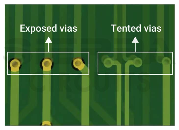
PCB via tenting protects vias from contamination, corrosion, and electrical shorts by covering exposed vias with a solder mask.| Sierra Circuits
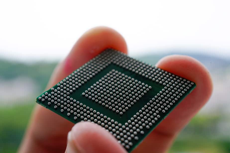
The BGA is the most popular package used in high I/O devices in the industry. It has a high lead (solder ball) count which is greater than 208 leads.| Sierra Circuits

Download the Design for Assembly Handbook from Sierra Circuits and explore the rest of our PCB design resources.| Sierra Circuits
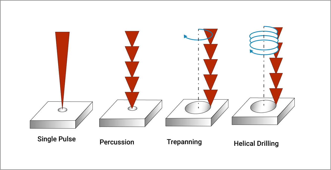
Laser drilling is performed to drill holes and vias on a PCB using a laser beam without compromising the board integrity.| Sierra Circuits
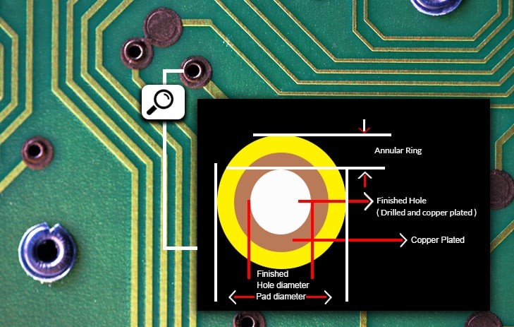
An annular ring is the copper area surrounding a plated via on a PCB. It establishes a solid connection between the via and copper traces.| Sierra Circuits
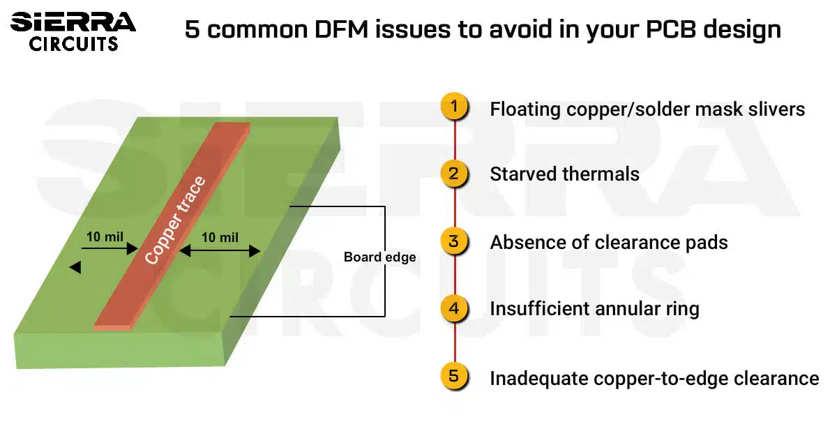
DFM checks each design before going for fabrication. It predicts potential defects and ensures board manufacturing with exact specifications.| Sierra Circuits

Download the Design for Manufacturing Handbook and learn the best design practices for your electronics in terms of both cost and complexity.| Sierra Circuits
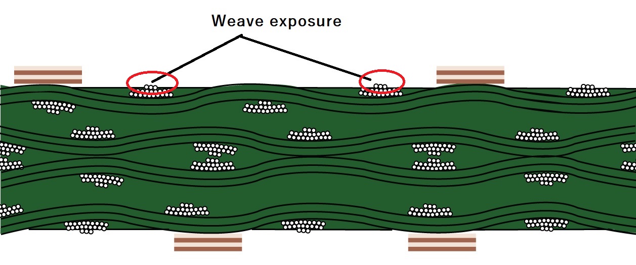
FR4 materials are widely used due to their cost-effectiveness, wide range of operating temperatures, and excellent thermal properties.| Sierra Circuits
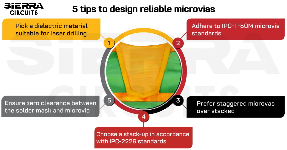
Design strategies for reliable microvias include selecting laser drillable materials and adhering to IPC-T-50M and IPC-2226 standards.| Sierra Circuits
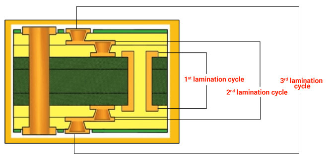
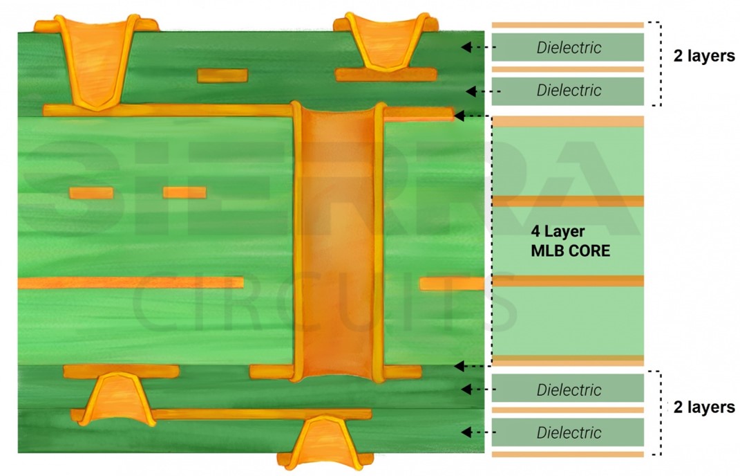
Sequential lamination is a process of fabricating a high-density PCB using cores and subsets composed of copper and dielectric layers.| Sierra Circuits
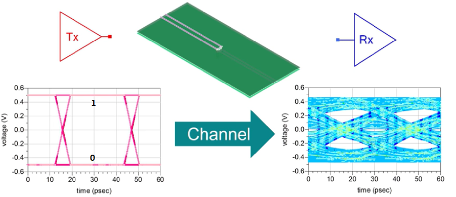
Signal integrity is the measurement of a signal’s quality when it propagates from the transmitter to the receiver in an electronic system.| Sierra Circuits
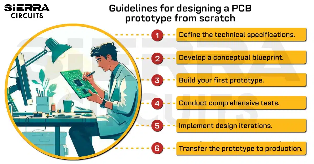
Designing a PCB prototype involves defining specifications, developing the system, testing, iterating, and validating with EVT samples.| Sierra Circuits
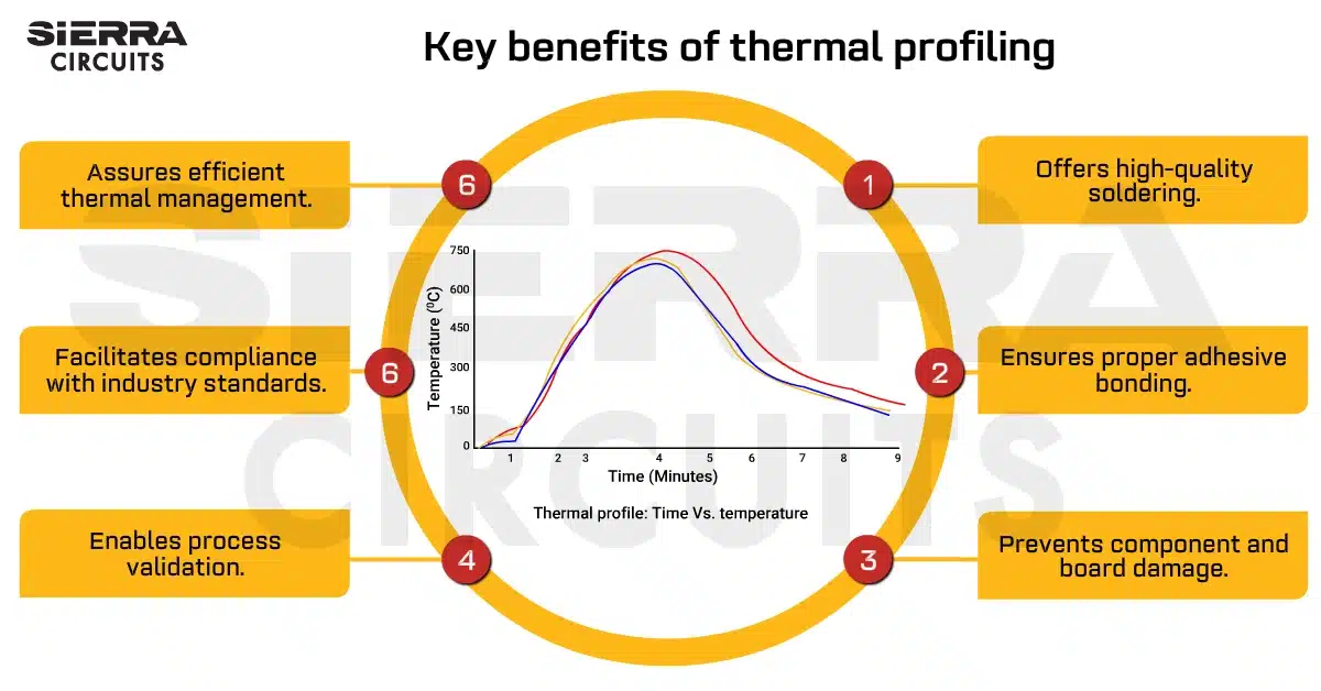
Thermal profiles capture the temperature changes a PCB undergoes during solder reflow or thermal curing, using sensors called thermocouples.| Sierra Circuits
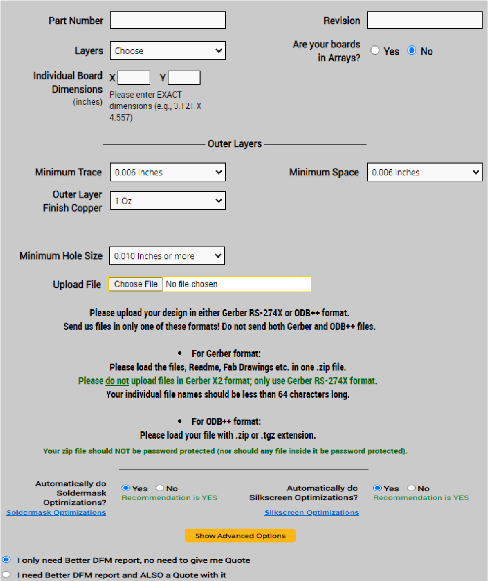
Better DFM is an online design tool that checks for the manufacturability of an electronic circuit design. Try it now!| Sierra Circuits
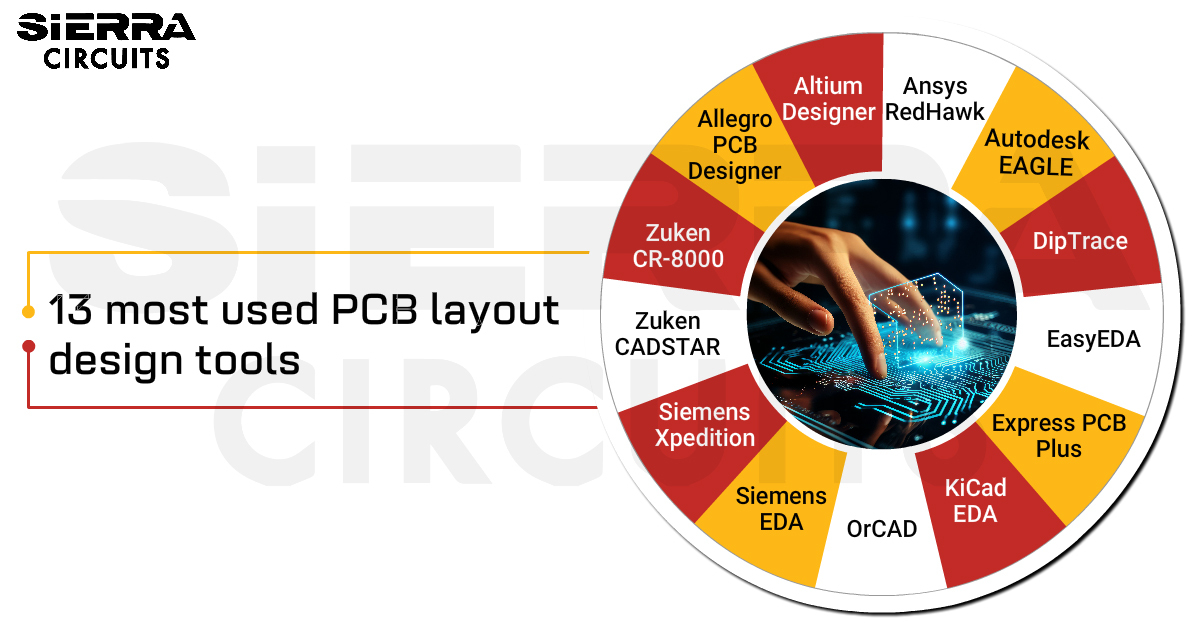
Some of the most used PCB layout design tools are Altium, Allegro, and KiCad. Consider UI, routing, and simulation before selecting one.| Sierra Circuits
Vias are miniature conductive pathways drilled into the PCB to establish electrical connectivity between the different layers.| Sierra Circuits
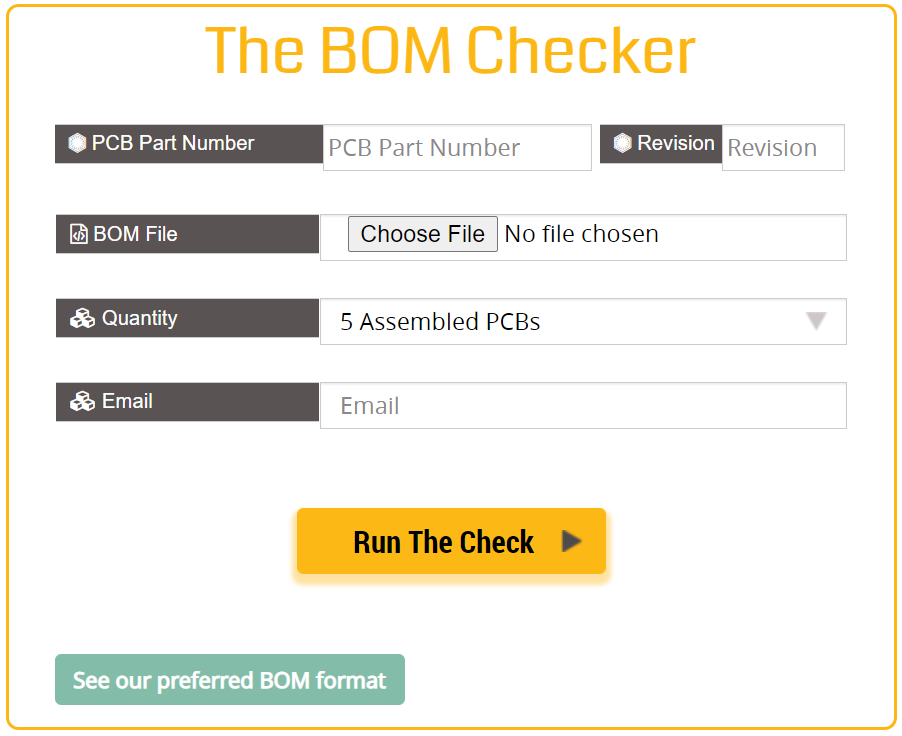
This BOM tool helps rectify the errors in the bill of materials list, get a cost estimation, and information regarding part availability.| Sierra Circuits
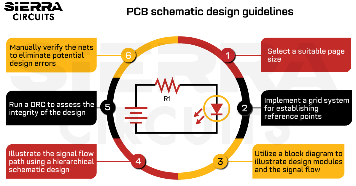
A PCB schematic must follow standard guidelines such as precision net labeling, and symbol standardization to have a well-structured design.| Sierra Circuits

Sierra Circuits builds your quickturn high-quality rigid PCB prototype. Contact our engineering team to learn about our PCB fab capabilities.| Sierra Circuits
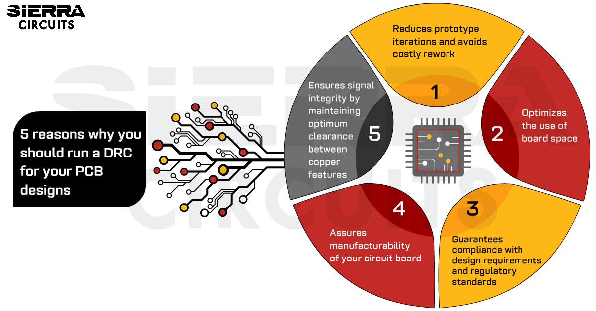
DRC helps you validate whether your PCB layout conforms to predefined constraints such as trace width, clearances, and hole sizes.| Sierra Circuits
