BGA: Features, Soldering, and X-Ray Inspection | Sierra Circuits
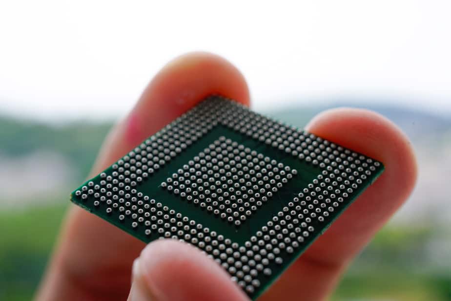
The BGA is the most popular package used in high I/O devices in the industry. It has a high lead (solder ball) count which is greater than 208 leads.| Sierra Circuits
The BGA is the most popular package used in high I/O devices in the industry. It has a high lead (solder ball) count which is greater than 208 leads.| Sierra Circuits

Learn about how thermal management techniques and thermal vias in PCB are essential to minimize heating issues and boost thermal performance.| Sierra Circuits
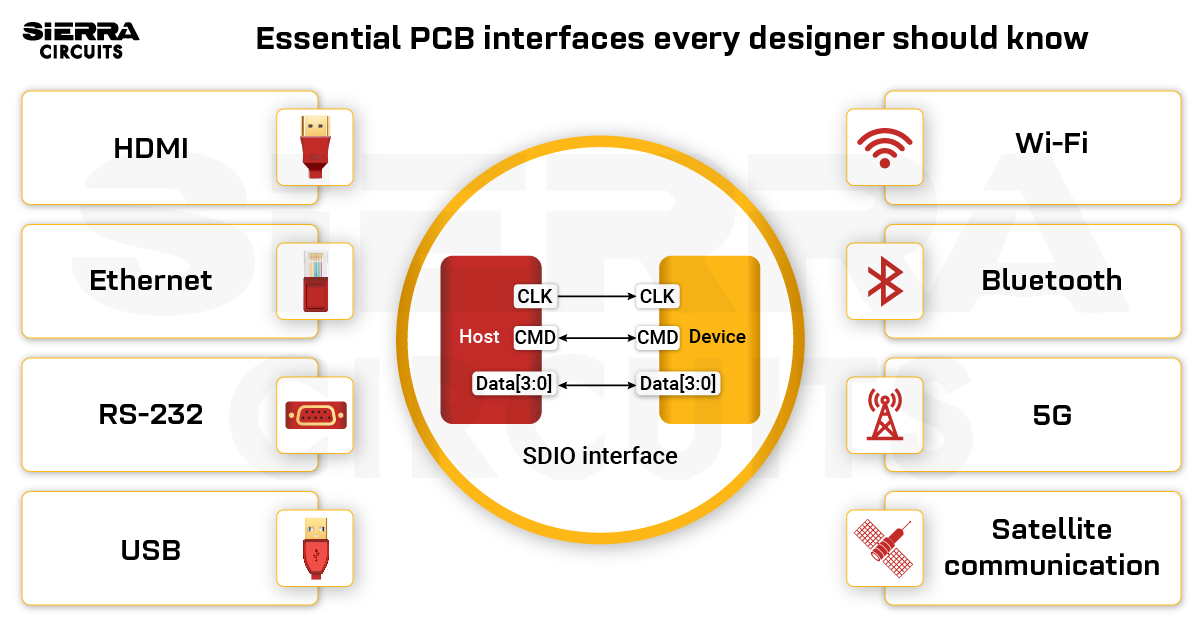
PCB interfaces are categorized into wired interfaces, like UART, I2C, and PCIe, and wireless interfaces, such as 5G, Wi-Fi, and LoRa.| Sierra Circuits

Download the Design for Assembly Handbook from Sierra Circuits and explore the rest of our PCB design resources.| Sierra Circuits
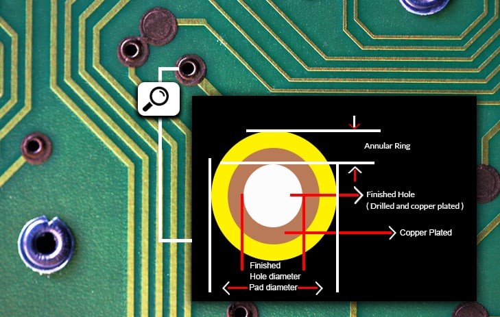
An annular ring is the copper area surrounding a plated via on a PCB. It establishes a solid connection between the via and copper traces.| Sierra Circuits

Download the Design for Manufacturing Handbook and learn the best design practices for your electronics in terms of both cost and complexity.| Sierra Circuits
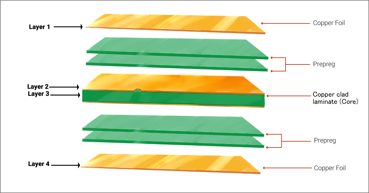
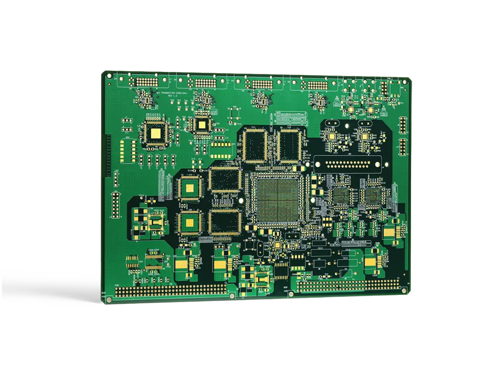
A multilayer PCB has more than two layers in its stack-up. The stack-up describes the construction of a multilayer board in sequential order.| Sierra Circuits
Sierra Circuits offers quickturn, high-quality, HDI printed circuit boards. Learn about our HDI PCB capabilities.| Sierra Circuits
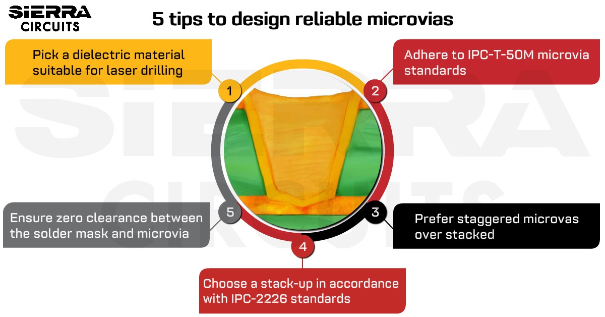
Design strategies for reliable microvias include selecting laser drillable materials and adhering to IPC-T-50M and IPC-2226 standards.| Sierra Circuits
Here are some best high-speed PCB routing practices that will help PCB designers to craft a perfect design.| Sierra Circuits
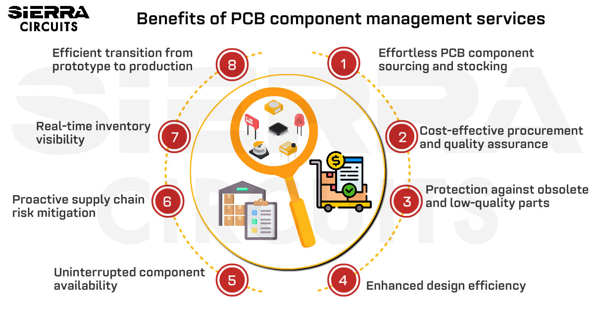
PCB component management services provide supply chain solutions by helping you procure, store, and manage high-quality parts.| Sierra Circuits
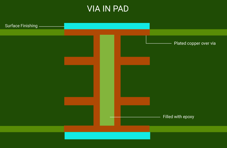
Use via-in-pad technology when the board size is limited, components have small footprints, and surface routing options are restricted.| Sierra Circuits
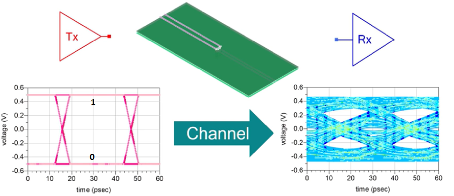
Signal integrity is the measurement of a signal’s quality when it propagates from the transmitter to the receiver in an electronic system.| Sierra Circuits
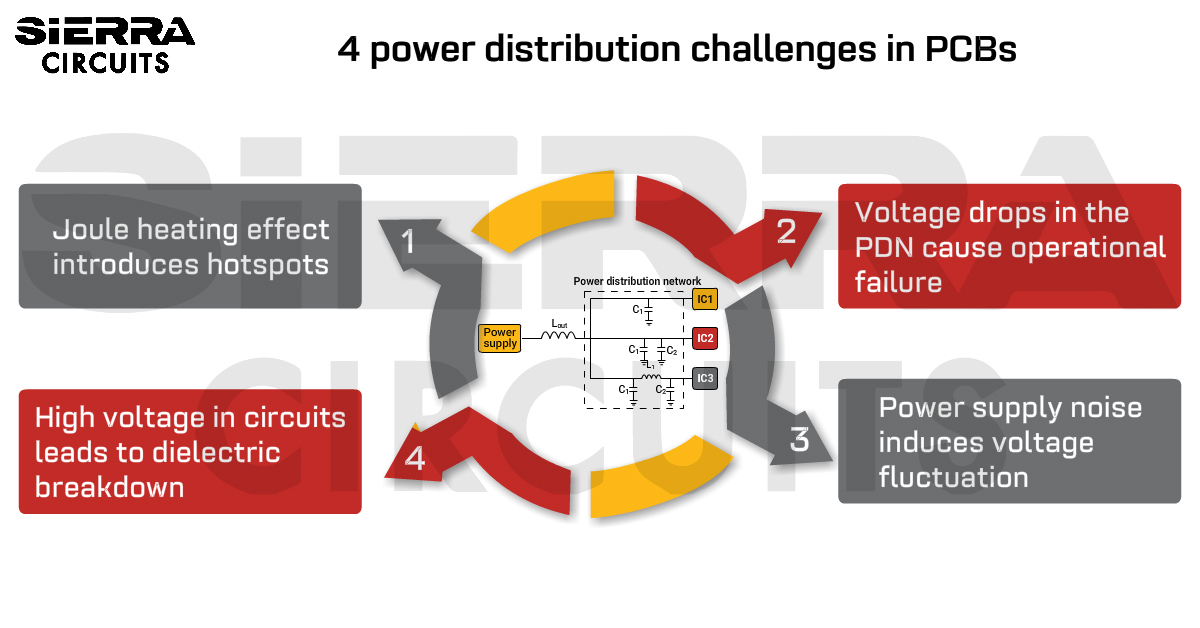
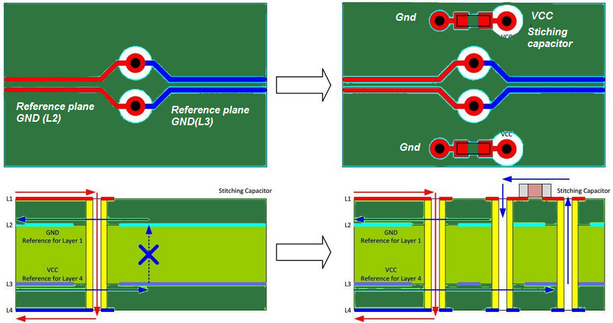
Employ decoupling capacitors, ferrite beads, and Faraday cages to suppress the power supply noise in your PDN design.| Sierra Circuits
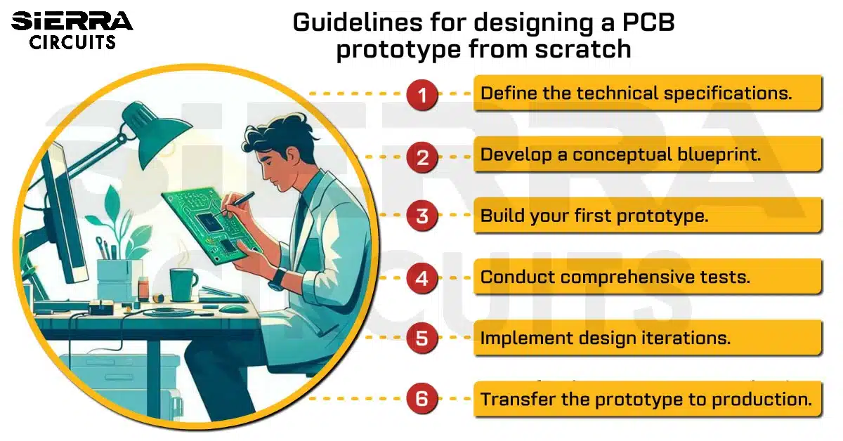
Designing a PCB prototype involves defining specifications, developing the system, testing, iterating, and validating with EVT samples.| Sierra Circuits
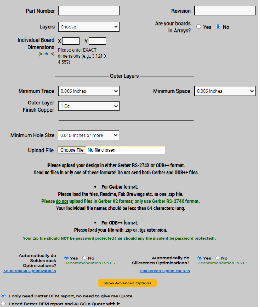
Better DFM is an online design tool that checks for the manufacturability of an electronic circuit design. Try it now!| Sierra Circuits

PCB fabrication considerations for proper component placement are essential to improve the signal quality and performance of your device.| Sierra Circuits
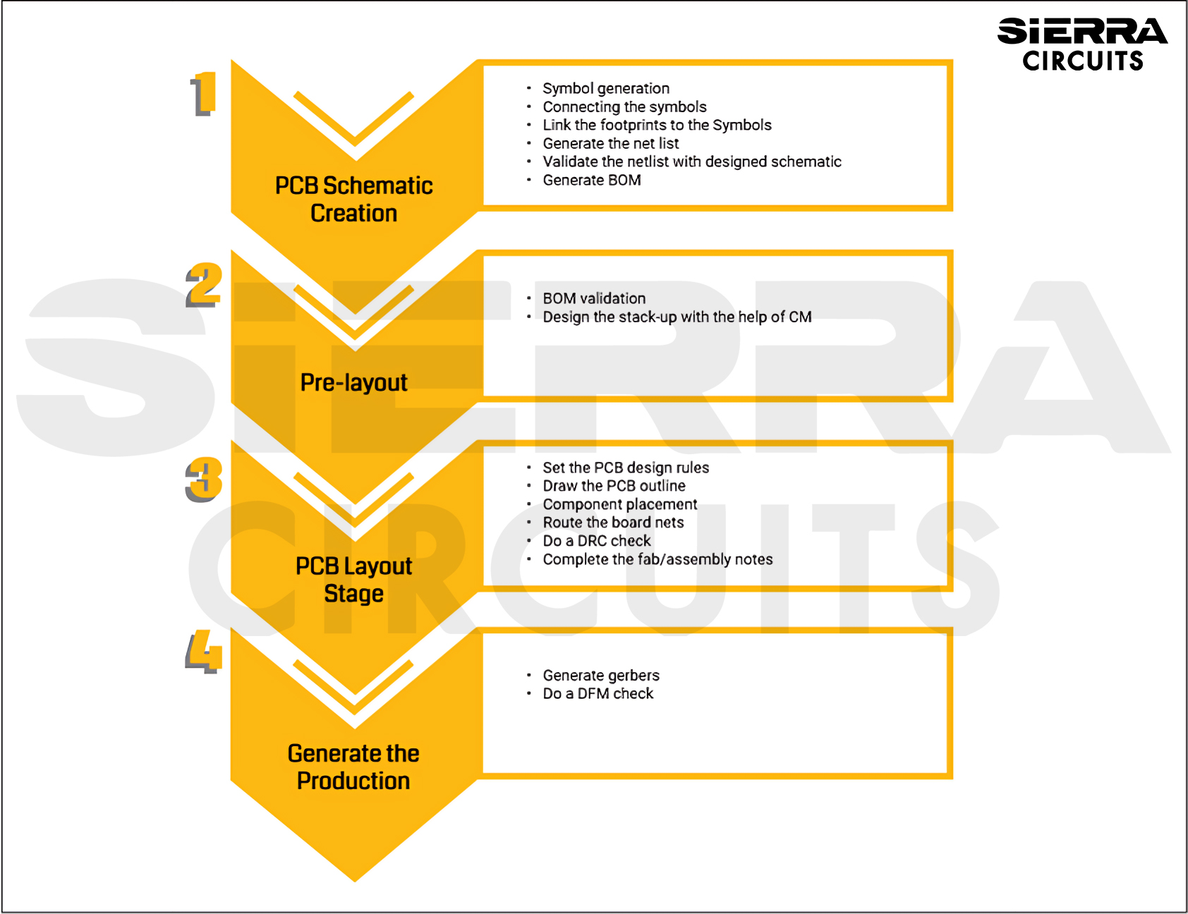
The PCB layout stage includes setting up the design tool, board outline, import of netlist, component placement, routing, silkscreen cleanup, and DRC check.| Sierra Circuits
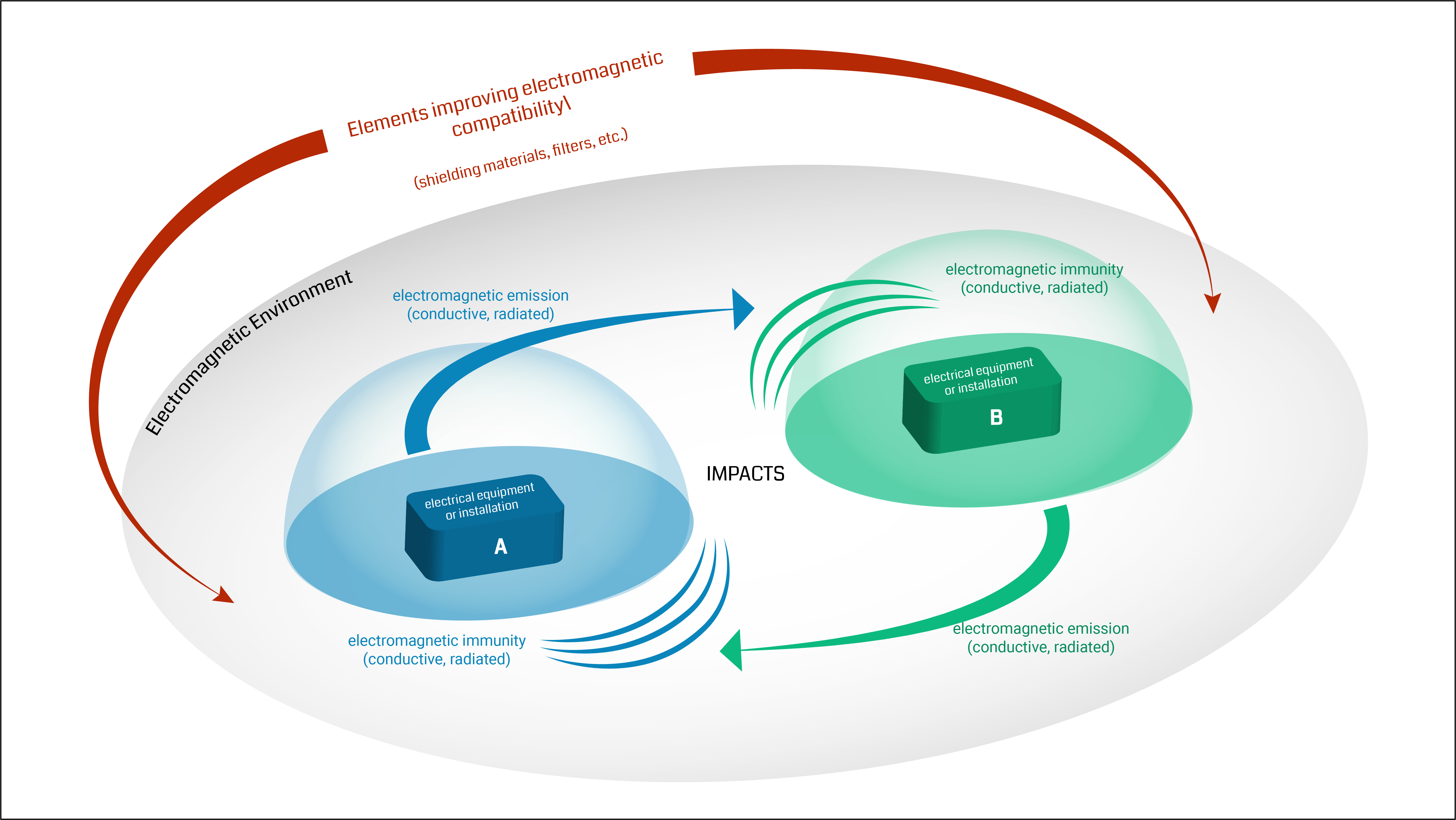
EMI can be mitigated by incorporating efficient grounding techniques and optimum trace spacing. This also ensures EMC.| Sierra Circuits
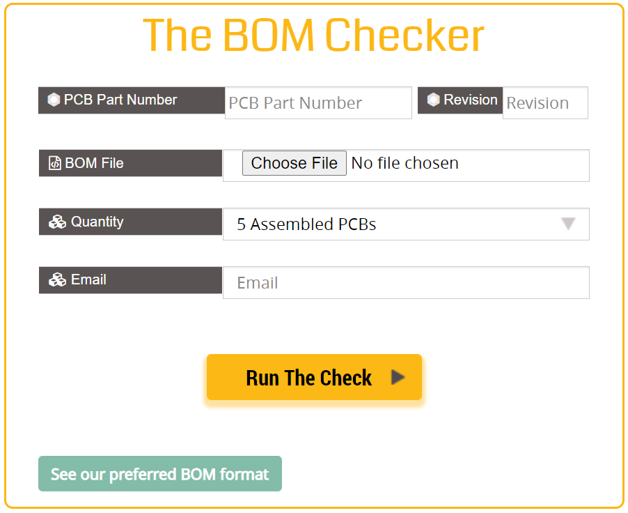
This BOM tool helps rectify the errors in the bill of materials list, get a cost estimation, and information regarding part availability.| Sierra Circuits
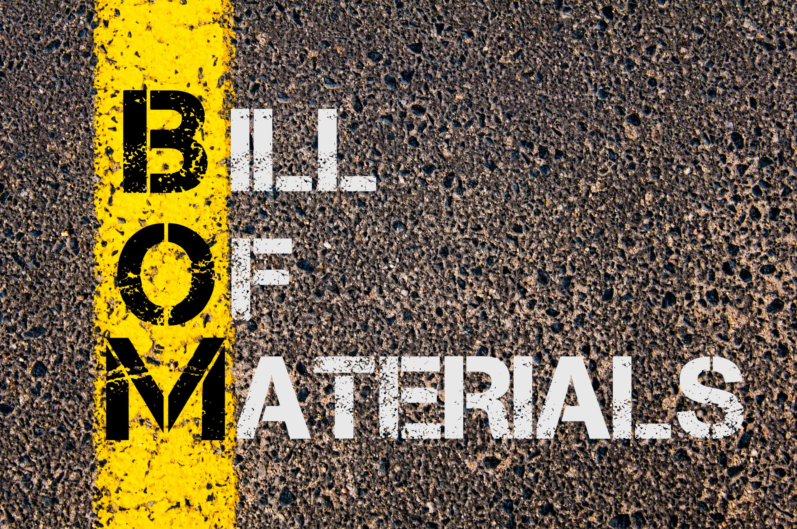
A PCB bill of materials (BOM) is a comprehensive list that provides information on all the components to be assembled on your board.| Sierra Circuits
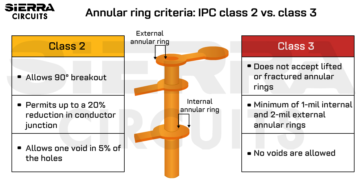
This article will help you understand the different PCB design rules for IPC Class 2 and Class 3 printed circuit boards.| Sierra Circuits
