PCB Component Sourcing and Stocking | Sierra Circuits
We handle your PCB component sourcing and stocking through effective component management to reduce your product development time. See how!| Sierra Circuits
We handle your PCB component sourcing and stocking through effective component management to reduce your product development time. See how!| Sierra Circuits
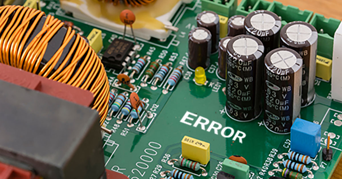
Common errors in discrete components occur due to voltage fluctuation, component aging, excessive heat, and corrosion.| Sierra Circuits

The Soldering Flux eBook by Jim Smith will teach you why nothing is more important than understanding flux selection and proper usage.| Sierra Circuits
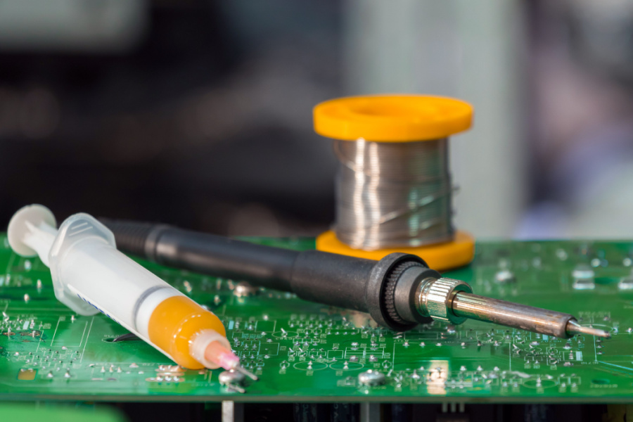
Flux selection may be the most important decision any electronics assembly business will ever make. Read this article by expert Jim Smith.| Sierra Circuits
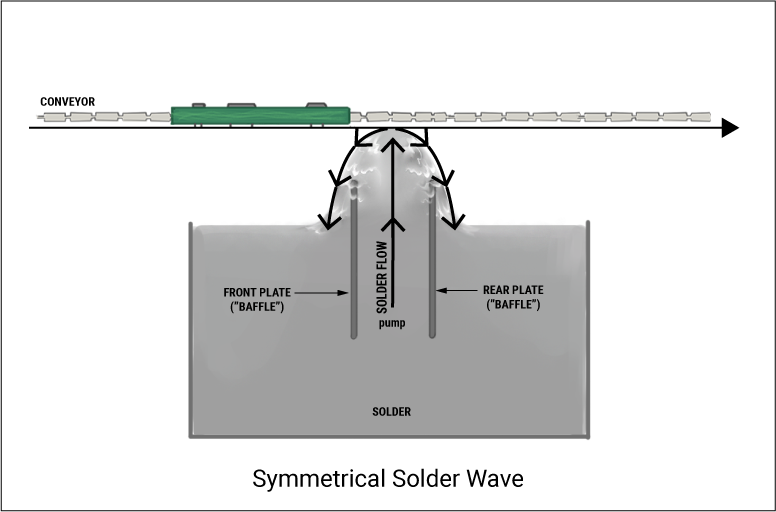
Wave soldering was the first practical automated mass soldering method for quickly soldering large numbers of components onto PCBs.| Sierra Circuits
J-STD-001 is a standard issued by IPC that defines material and process requirements for soldered electrical and electronic assemblies.| Sierra Circuits
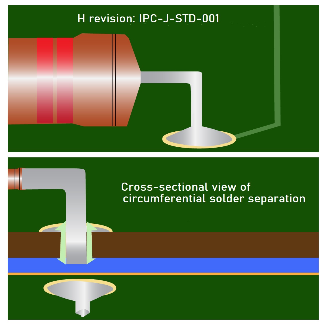
The H revision of soldering standards provides clarification on assembly considerations like toe overhang, and cleaning requirements.| Sierra Circuits

Here are some soldering tips that, while very important, do not require hundreds of words each. These are the basis to master the solder iron techniques.| Sierra Circuits
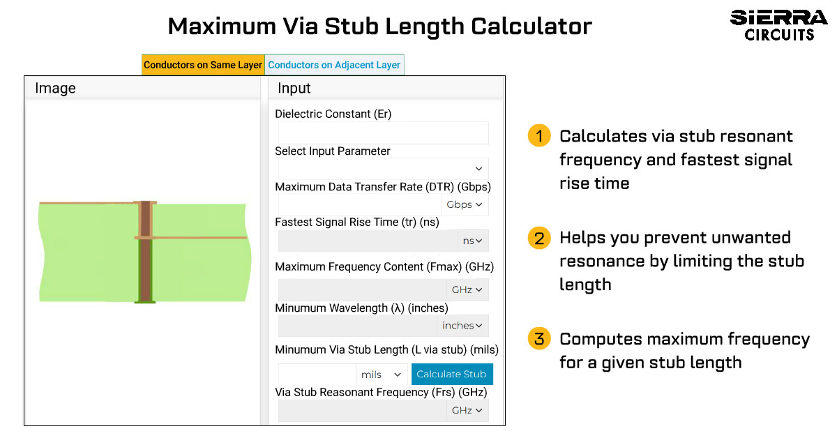
Sierra Circuits' Maximum Via Stub Length Calculator calculates the maximum length and resonant frequency of a via stub.| Sierra Circuits
Avoiding signal integrity issues in a PCB is a complex task for designers. It requires a deep understanding of design rules and techniques.| Sierra Circuits
In this article, we will go over the fundamentals of via design using Altium Designer electronic design automation software.| Sierra Circuits
Signal attenuation is the measure of the reduction in signal strength. It can be controlled by adopting repeaters, amplifiers, and materials| Sierra Circuits

Watch our webinar on understanding high-speed digital design to optimize signal integrity on PCBAs by Mike Resso of Keysight.| Sierra Circuits
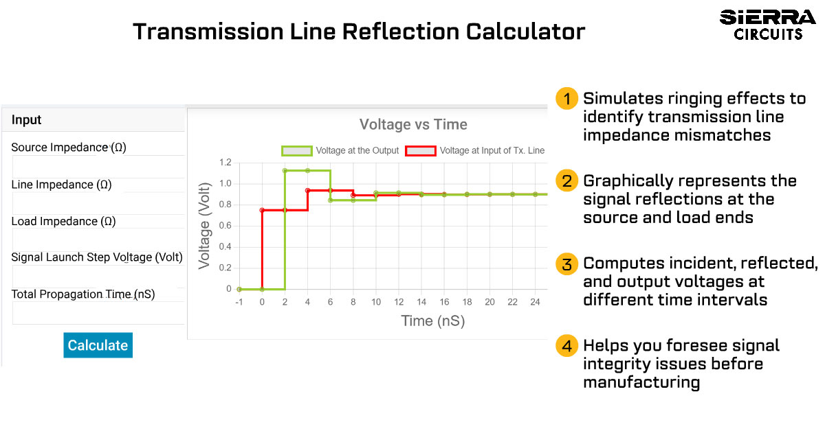
Sierra Circuits Transmission Line Reflection Calculator graphically displays the ringing of a signal in the transmission line.| Sierra Circuits
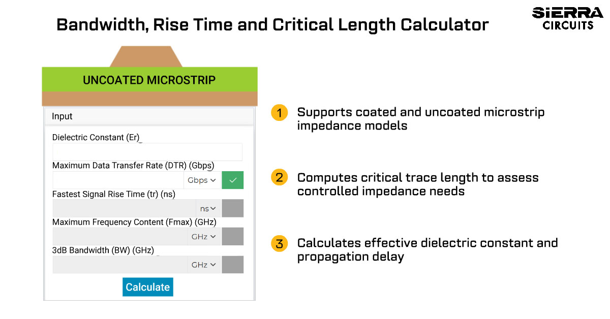
The Bandwidth, Rise Time, and Critical Length Calculator helps compute and analyze high-speed trace parameters to avoid signal distortion.| Sierra Circuits
Sierra Circuits manufactures high-quality RF PCBs and microwave prototypes with PTFE and non-PTFE materials to achieve signal integrity.| Sierra Circuits
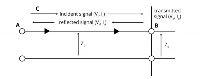
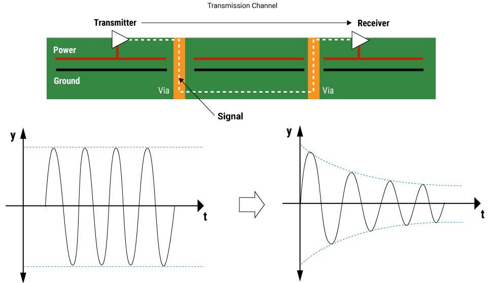
We previously discussed impedance discontinuity and signal reflection in our PCB transmission line series. Reflections occur due to impedance discontinuity.| Sierra Circuits
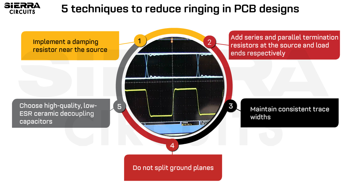
To reduce PCB ringing, implement a damping resistor at the source and maintain uniform trace width and spacing throughout the signal line.| Sierra Circuits
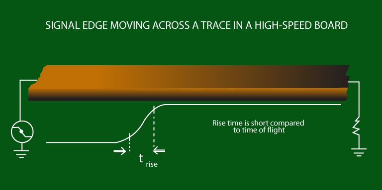
High clock frequencies and decreased rise times are some of the effects of high-speed signals in a PCB design, leading to signal degradation.| Sierra Circuits
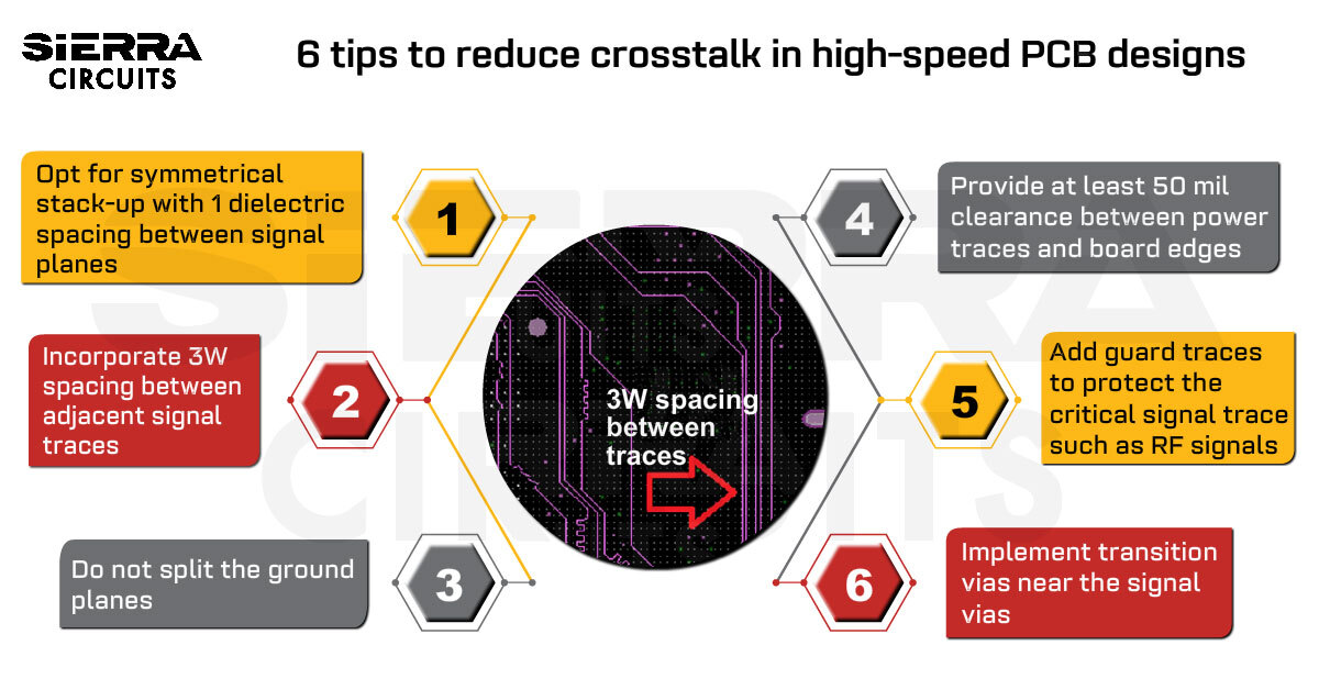
Crosstalk can be reduced in high-speed PCB designs by implementing 3W spacing between signal lines, guard traces, and solid ground planes.| Sierra Circuits
Sierra Circuits Canada was established in 2022 to service the PCB manufacturing and assembly needs of our Canadian and worldwide customers.| Sierra Circuits
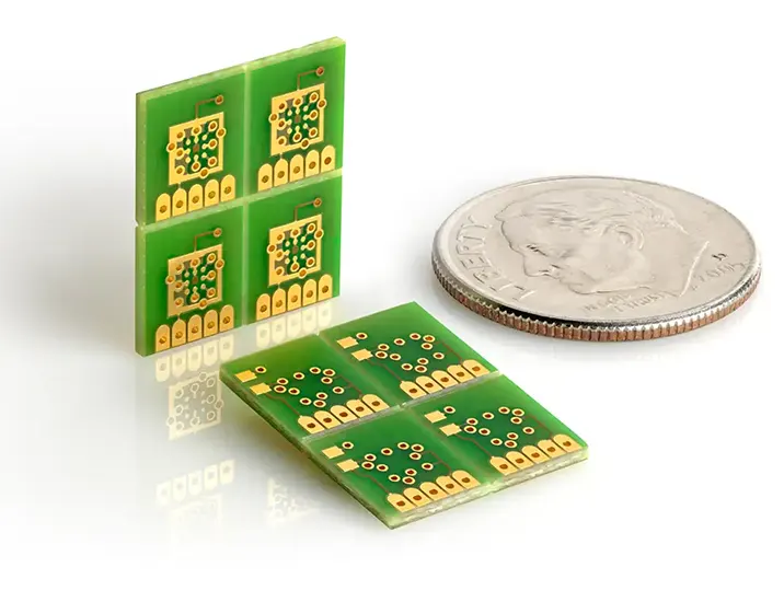
Sierra Circuits’ high-quality microelectronics PCBs. Speak to a microelectronic PCB specialist about manufacturing small circuit boards.| Sierra Circuits
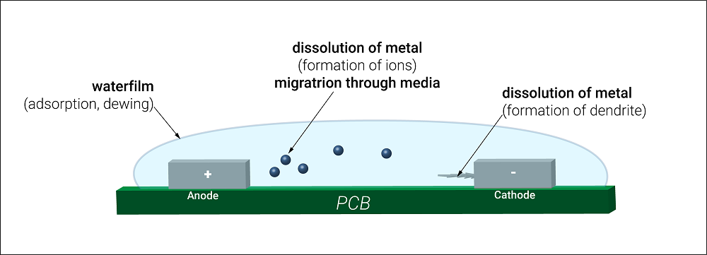
Did you know that more than 25% of PCB failures occur due to ionic contamination? Learn how to avoid issues with your board.| Sierra Circuits
Laurent Nicole shares his insights about the future of PCB etching and advanced technologies such as plasma and sputtering.| Sierra Circuits
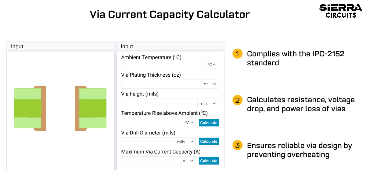
Try this user-friendly via current capacity and temperature rise calculator to obtain values of important via design parameters.| Sierra Circuits
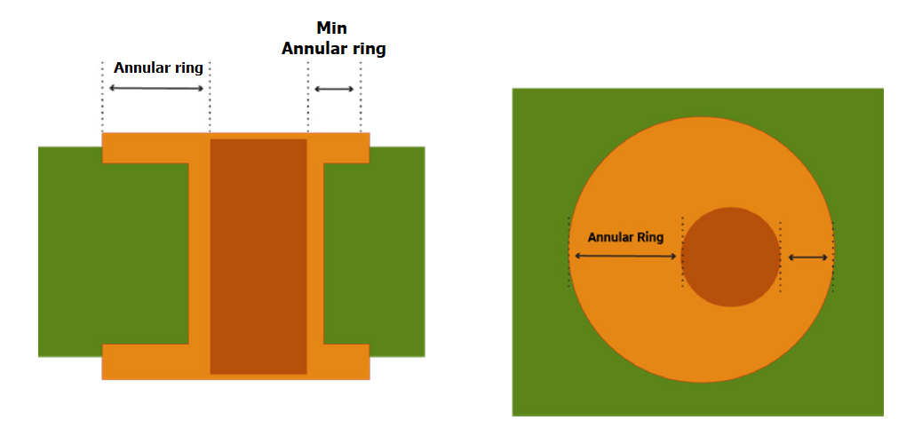
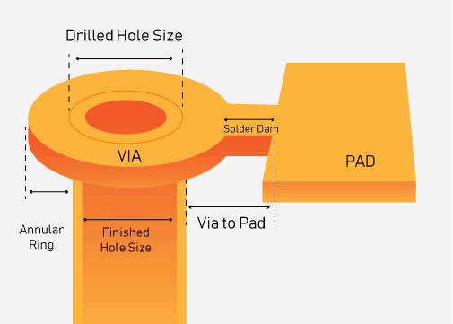
The minimum annular ring size should be greater than or equal to the values defined in the PCB design.| Sierra Circuits
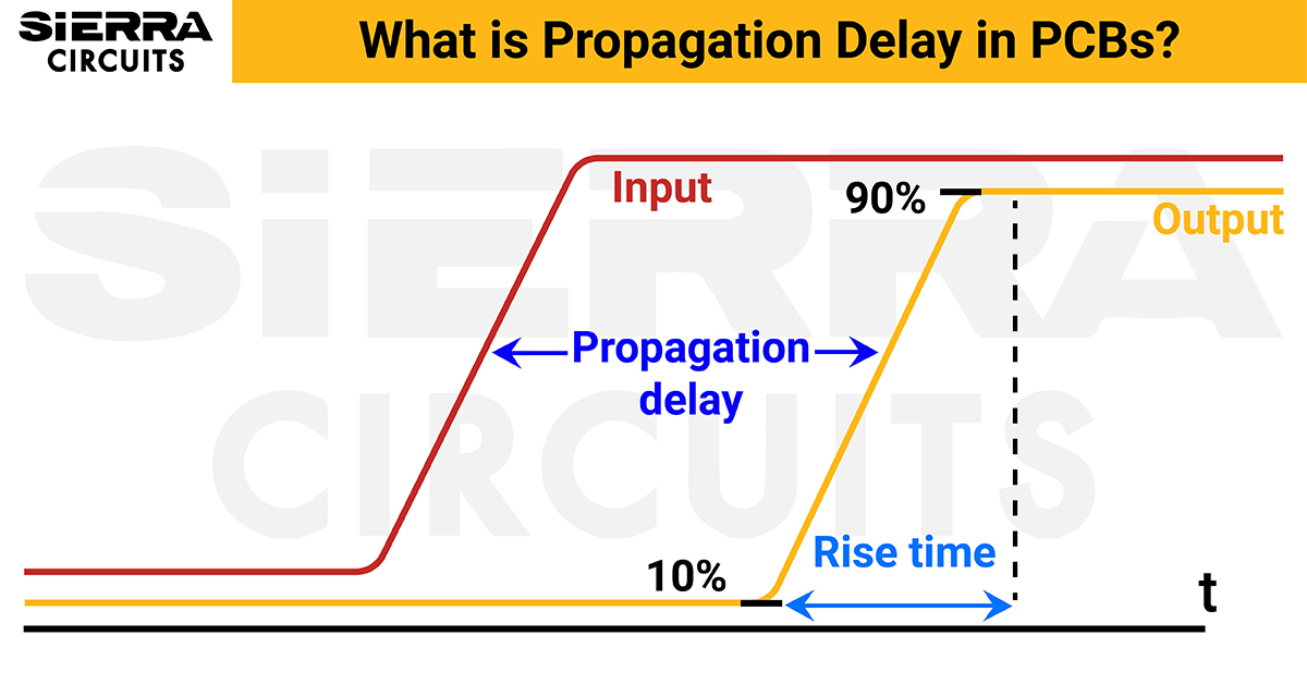
Propagation delay (tpd) in PCBs is the time taken by a signal to travel through a unit length of a transmission line.| Sierra Circuits
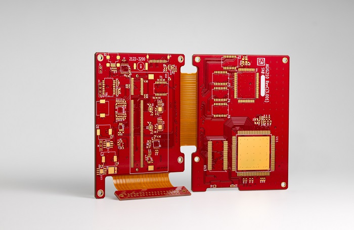
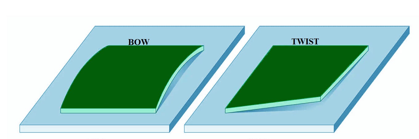
Rigid-flex PCB designs may be expensive to fabricate, but they can essentially save costs during electronic system assembly.| Sierra Circuits
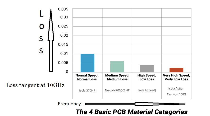
Proper PCB material selection is important since it affects the electrical performance of the signal traces.| Sierra Circuits
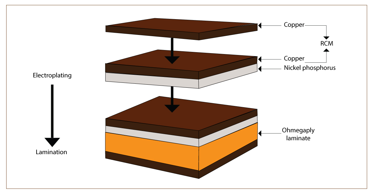
OhmegaPly and TCR follow the embedded passives technology that manufactures components like resistors and capacitors into the PCB substrate.| Sierra Circuits
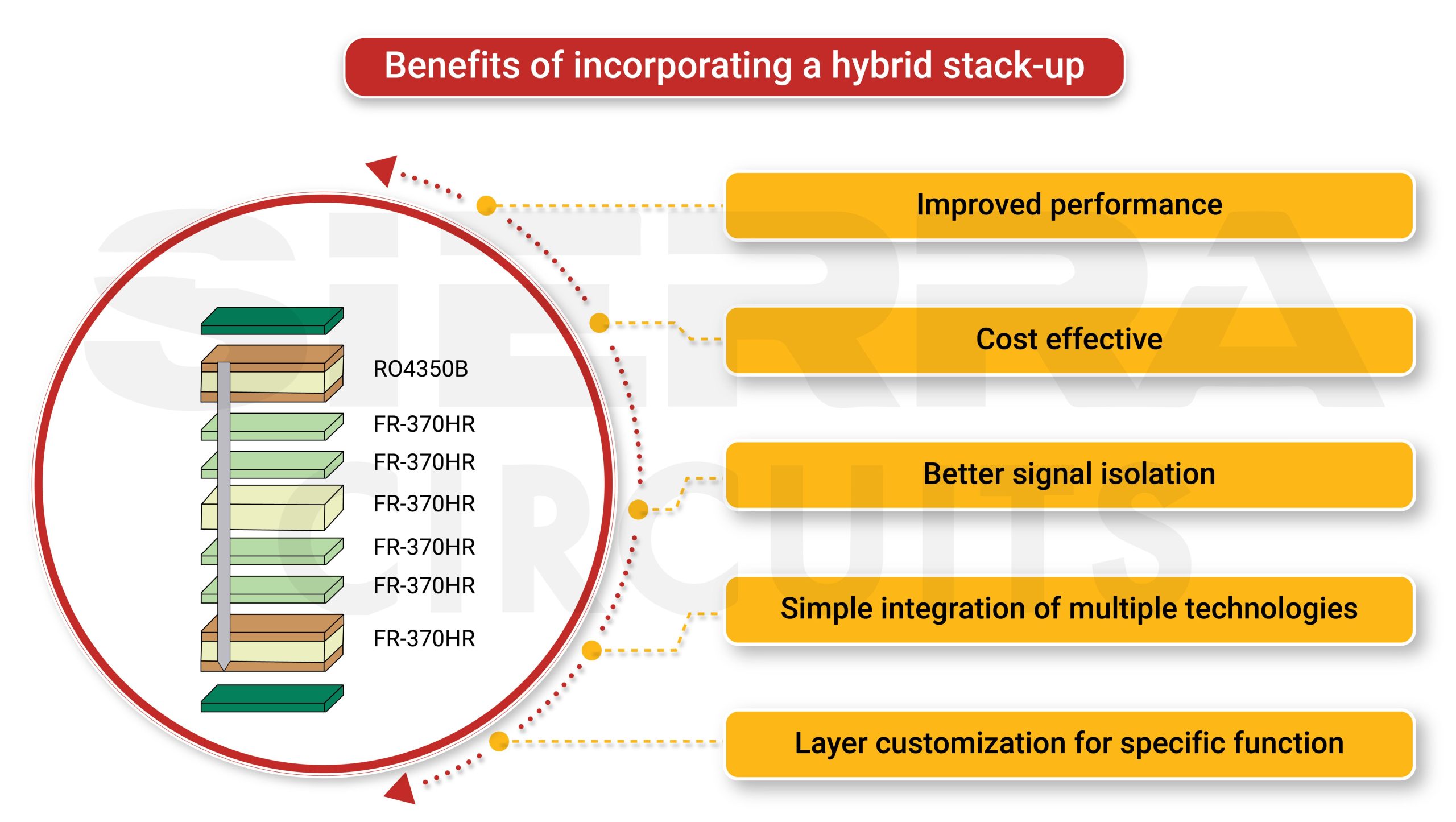
A hybrid stackup is built using a combination of dielectric materials to improve the PCB's performance and cost-effectiveness.| Sierra Circuits
Manufacturing controlled impedance PCBs requires due attention to dielectric material and trace width, height, thickness, and stack-up arrangement.| Sierra Circuits

Welcome to Sierra Circuits, your go-to solution for top-tier electronics, offering online PCB manufacturing and assembly quotes.| Sierra Circuits
The PCB Stack-Up Design Guide helps you build efficient stack-ups with improved SI, power distribution, and heat dissipation. Download now!| Sierra Circuits
PCB layer count estimation is a critical step to achieving design success as it directly impacts the functional capability of your board.| Sierra Circuits
Balanced copper distribution in your PCB design can be achieved by incorporating copper thieving and hatch patterns.| Sierra Circuits
Sierra Circuits Canada was established in 2022 to service the PCB manufacturing and assembly needs of our Canadian and worldwide customers.| Sierra Circuits
Sierra Circuits offers high tech pcb manufacturing and assembly on fast turnaround. Receive instant quote and order your PCBs online.| www.protoexpress.com
Sierra Circuits Canada was established in 2022 to service the PCB manufacturing and assembly needs of our Canadian and worldwide customers.| Sierra Circuits
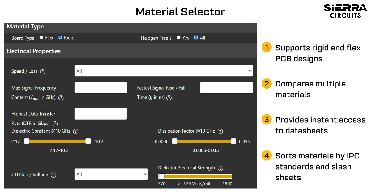
Use this PCB material selector before you send your design to manufacturing and find materials that suit your application. Try it now!| Sierra Circuits
Sierra Circuits offers one-stop PCB assembly services in our Silicon Valley location. Get a quote today for your PCBA needs.| Sierra Circuits
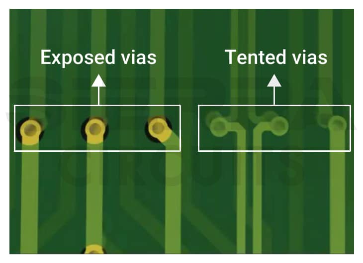
PCB via tenting protects vias from contamination, corrosion, and electrical shorts by covering exposed vias with a solder mask.| Sierra Circuits
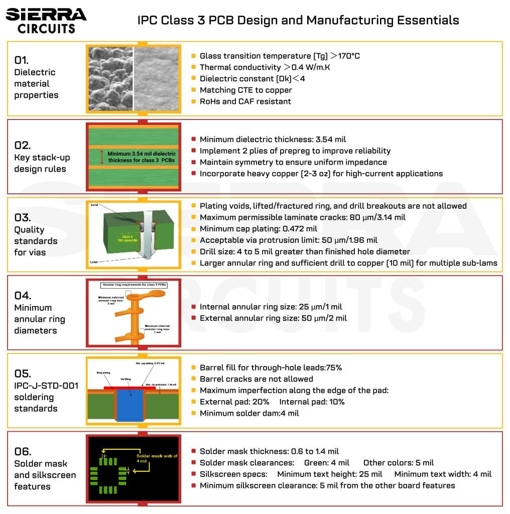
To build an efficient class 3 PCB, you need to design your stack-up, annular ring, and vias as per the IPC-6012 and IPC-A-610 standards.| Sierra Circuits
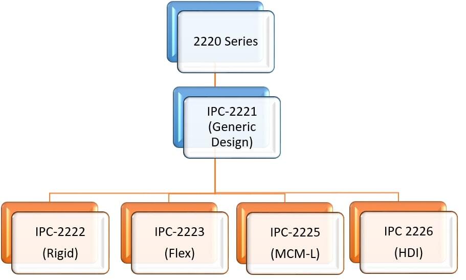
IPC-2221 is a standard that lays down the requirements for material selection, component placement, and high-voltage spacing requirements.| Sierra Circuits
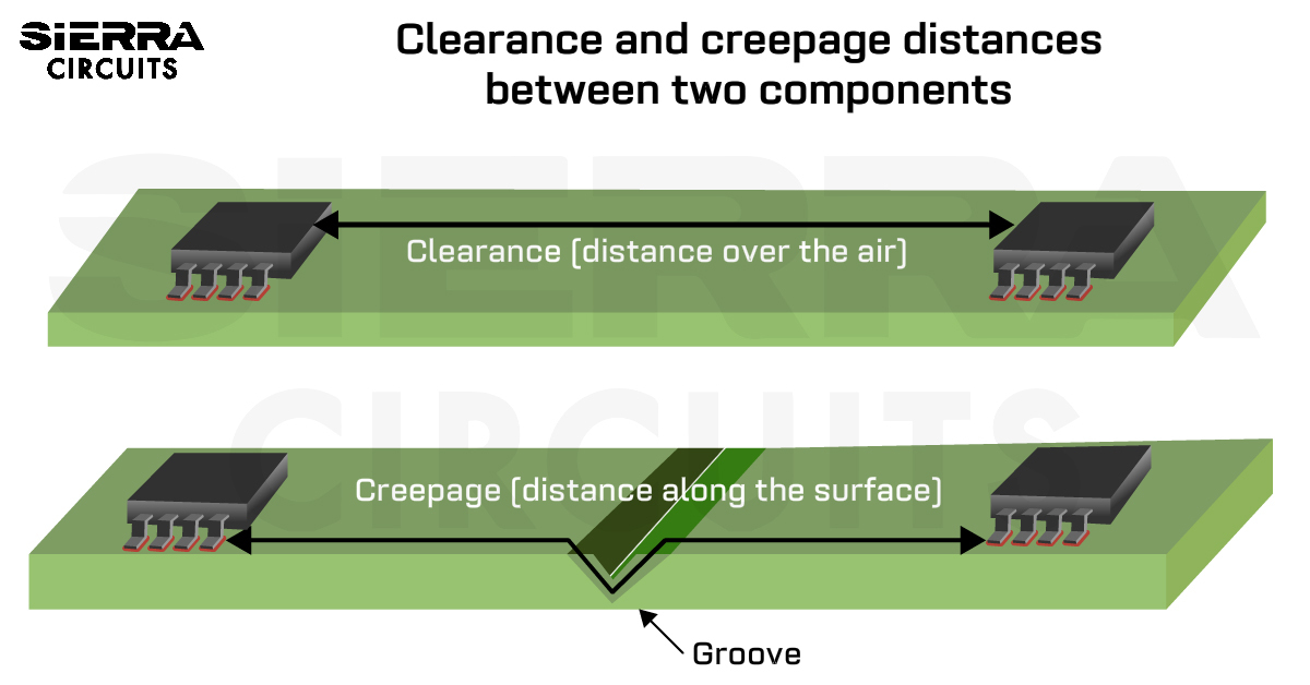
PCB creepage and clearances depend on CTI, pollution degree, working voltage, insulation, and altitude of the system.| Sierra Circuits
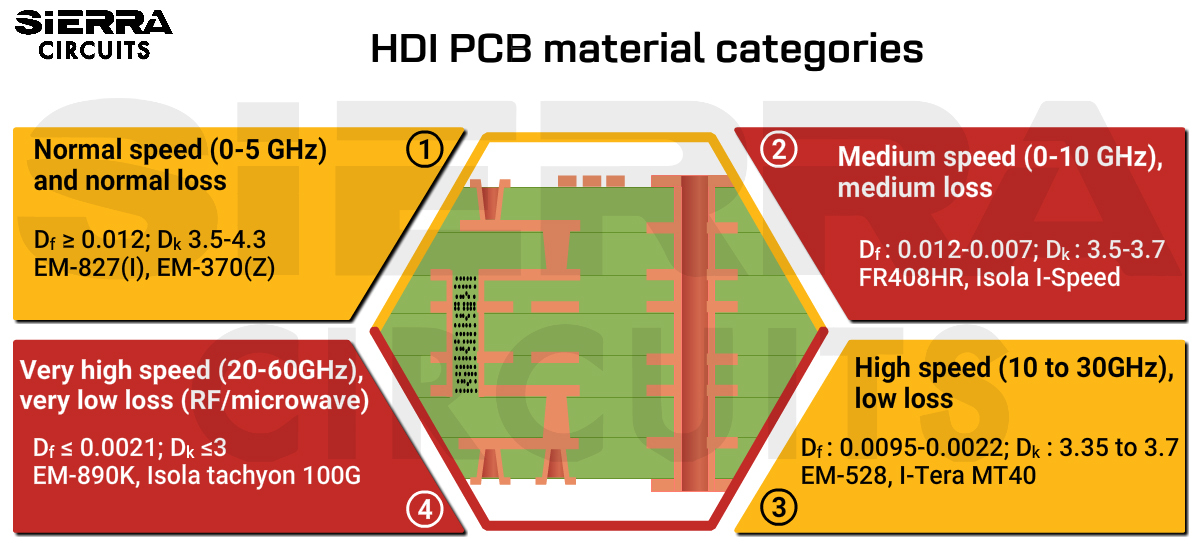
When choosing HDI PCB material, consider the operating frequency, acceptable signal loss, and laser drilling compatibility.| Sierra Circuits

Sierra Circuits Canada was established in 2022 to service the PCB manufacturing and assembly needs of our Canadian and worldwide customers.| Sierra Circuits
Sierra Circuits Canada was established in 2022 to service the PCB manufacturing and assembly needs of our Canadian and worldwide customers.| Sierra Circuits
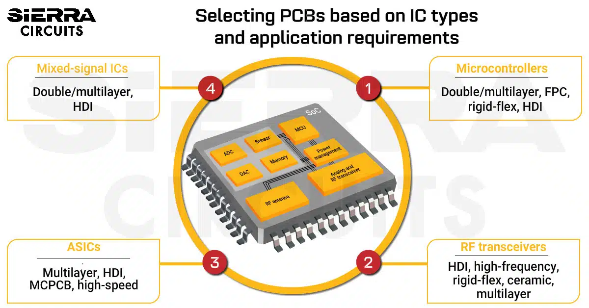
Selecting the right PCBs for IC integration depends on the chip’s signal characteristics, power demands, and the end-product.| Sierra Circuits
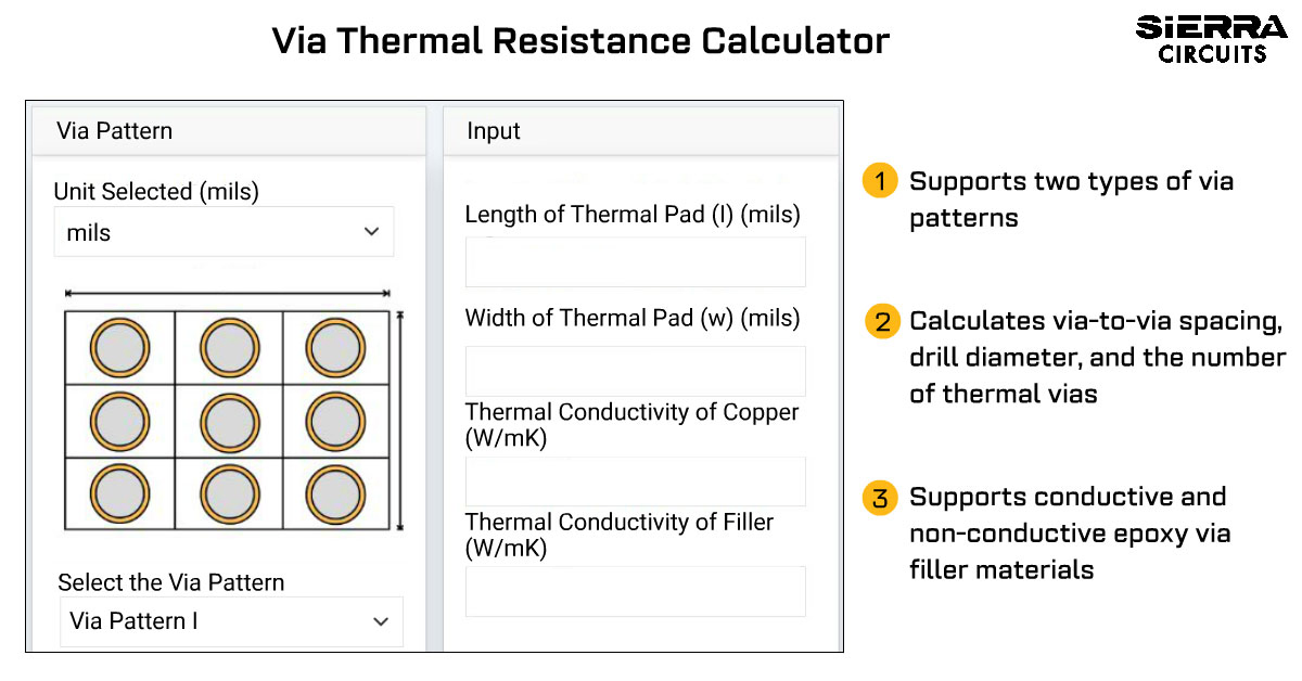
Sierra Circuits' Via Thermal Resistance Calculator computes the thermal resistance of a single or a combination of vias.| Sierra Circuits
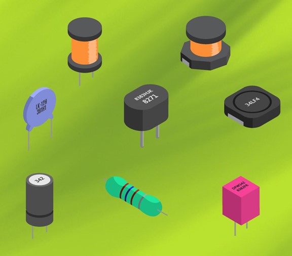
Passive and active electronic components like capacitors and inductors are available in standardized packages that designers can choose.| Sierra Circuits
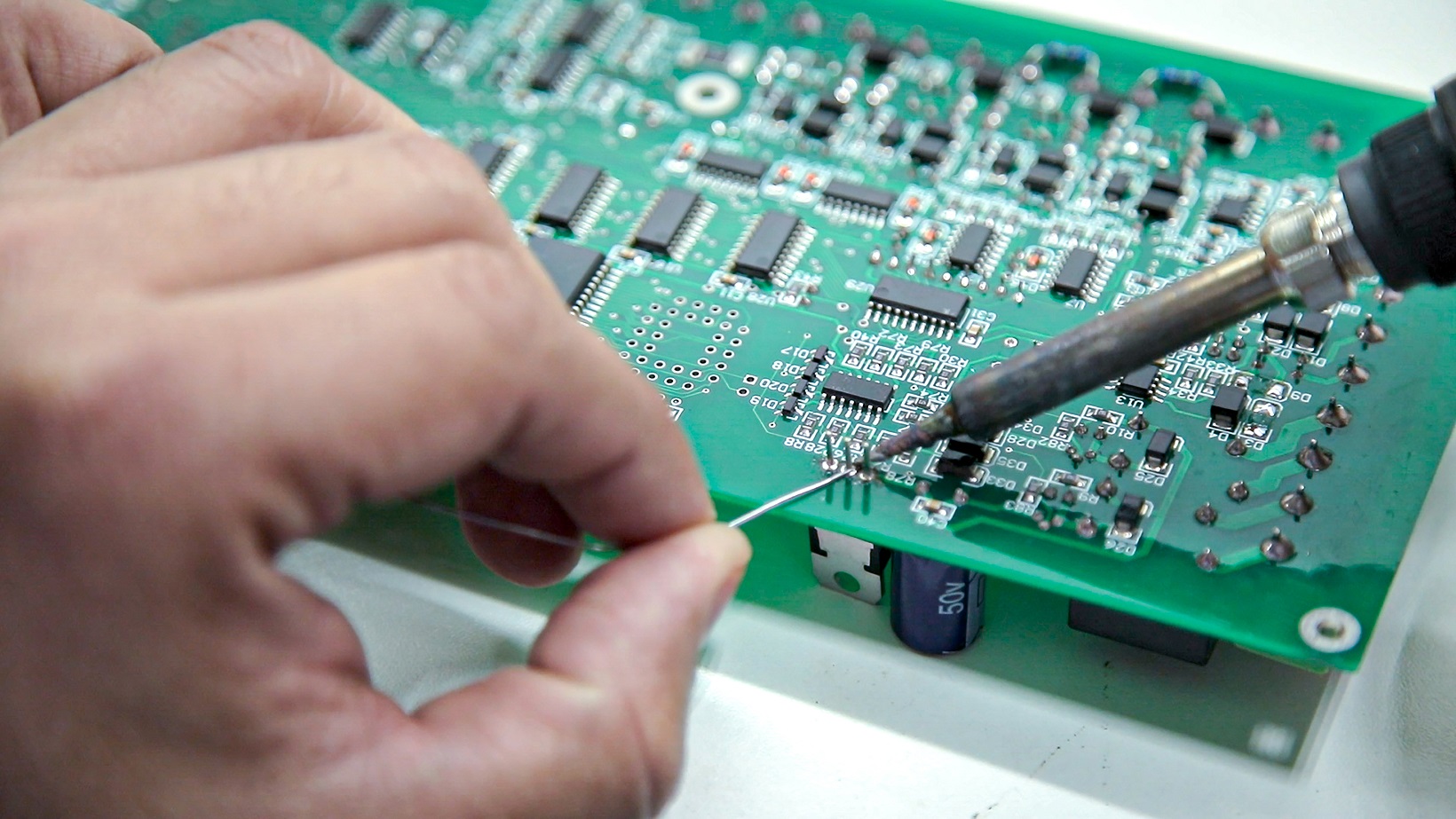
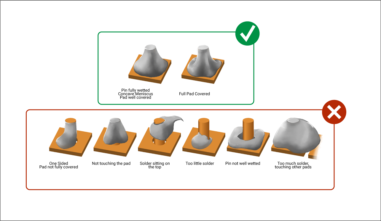
PCB soldering is the core process of electronics assembly, few people know how to solder reliably and often become proficient at hiding defects.| Sierra Circuits
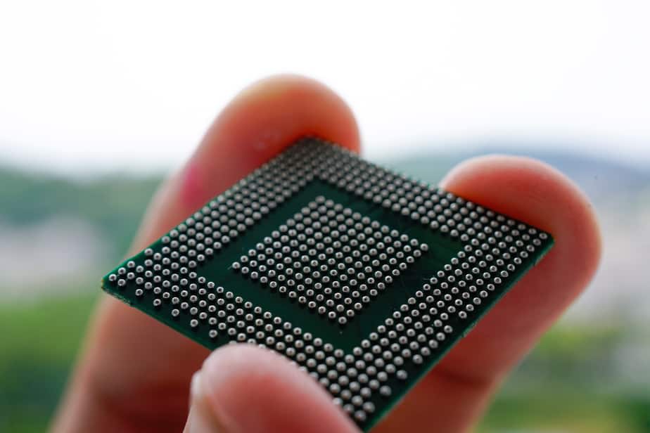
The BGA is the most popular package used in high I/O devices in the industry. It has a high lead (solder ball) count which is greater than 208 leads.| Sierra Circuits
Learn about how thermal management techniques and thermal vias in PCB are essential to minimize heating issues and boost thermal performance.| Sierra Circuits
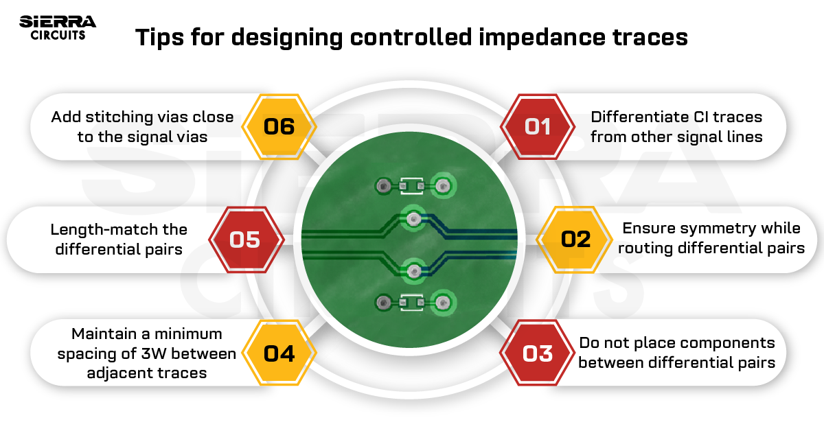
PCB materials, dielectric constant, trace height, and width affect the controlled impedance of a transmission line.| Sierra Circuits
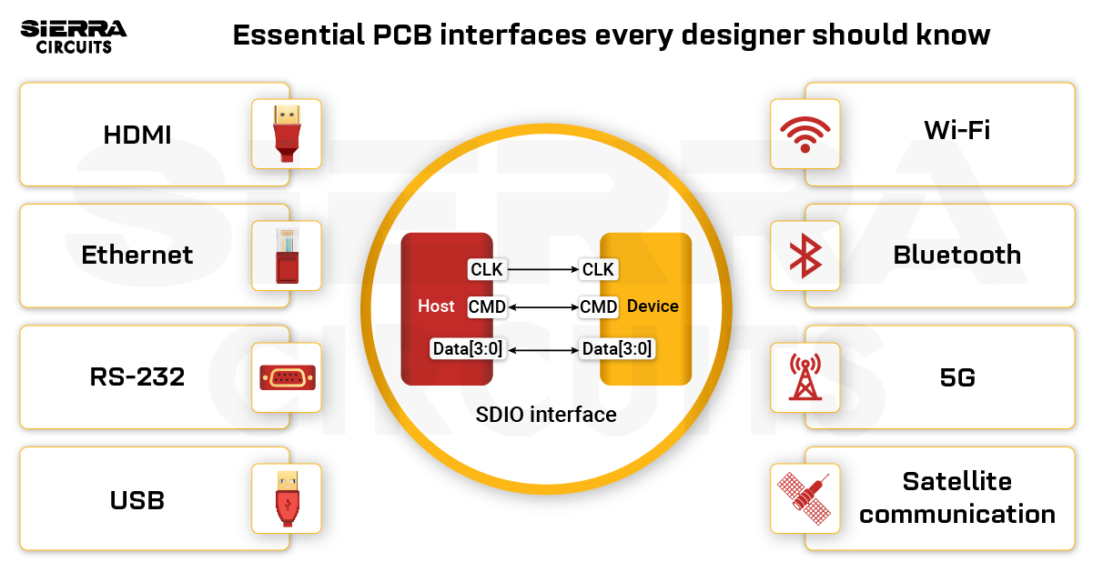
PCB interfaces are categorized into wired interfaces, like UART, I2C, and PCIe, and wireless interfaces, such as 5G, Wi-Fi, and LoRa.| Sierra Circuits

Download the Design for Assembly Handbook from Sierra Circuits and explore the rest of our PCB design resources.| Sierra Circuits
PCB assembly process involves DFA, SMT and through-hole components placement, testing, and final inspection.| Sierra Circuits
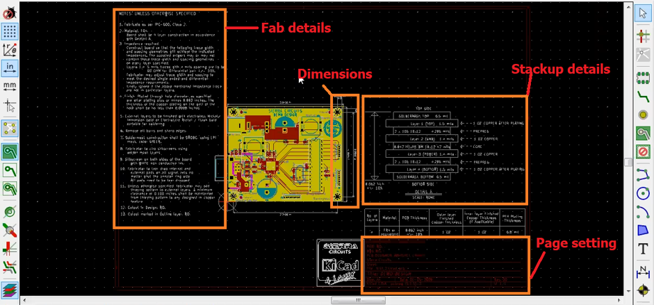
A PCB fab drawing is a reference document for manufacturing and includes all the information like board outline, stack-up, drilled holes, etc.| Sierra Circuits
Computer-Aided Manufacturing for PCBs is the use of software and computer-controlled machinery to perform tasks like drilling and component insertion.| Sierra Circuits
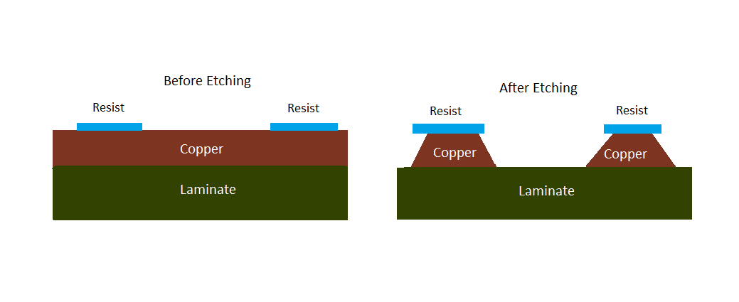
Wet PCB etching is a process of removing unwanted copper by immersing a circuit board in a chemical solution (acidic or alkaline based).| Sierra Circuits
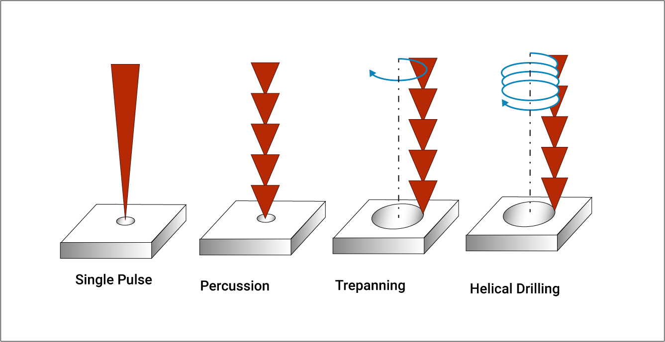
Laser drilling is performed to drill holes and vias on a PCB using a laser beam without compromising the board integrity.| Sierra Circuits
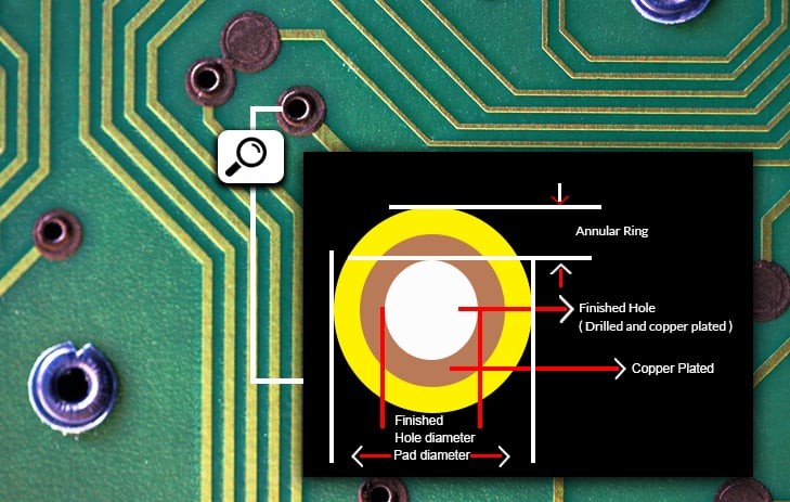
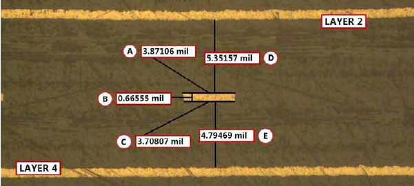
An annular ring is the copper area surrounding a plated via on a PCB. It establishes a solid connection between the via and copper traces.| Sierra Circuits
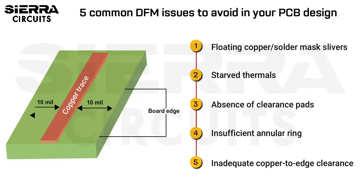
DFM checks each design before going for fabrication. It predicts potential defects and ensures board manufacturing with exact specifications.| Sierra Circuits
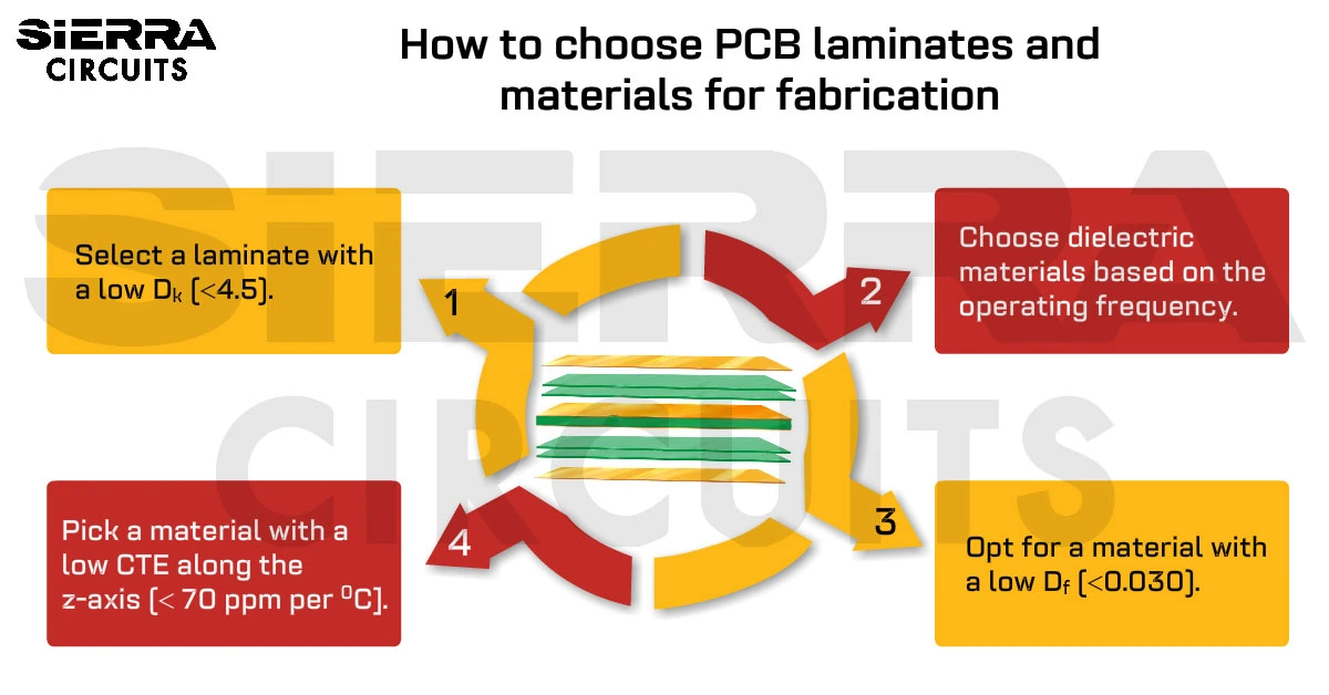
Selecting the right PCB laminates and materials for your design is very important as it can impact the overall performance of the board.| Sierra Circuits

Download the Design for Manufacturing Handbook and learn the best design practices for your electronics in terms of both cost and complexity.| Sierra Circuits
FR4 materials are widely used due to their cost-effectiveness, wide range of operating temperatures, and excellent thermal properties.| Sierra Circuits
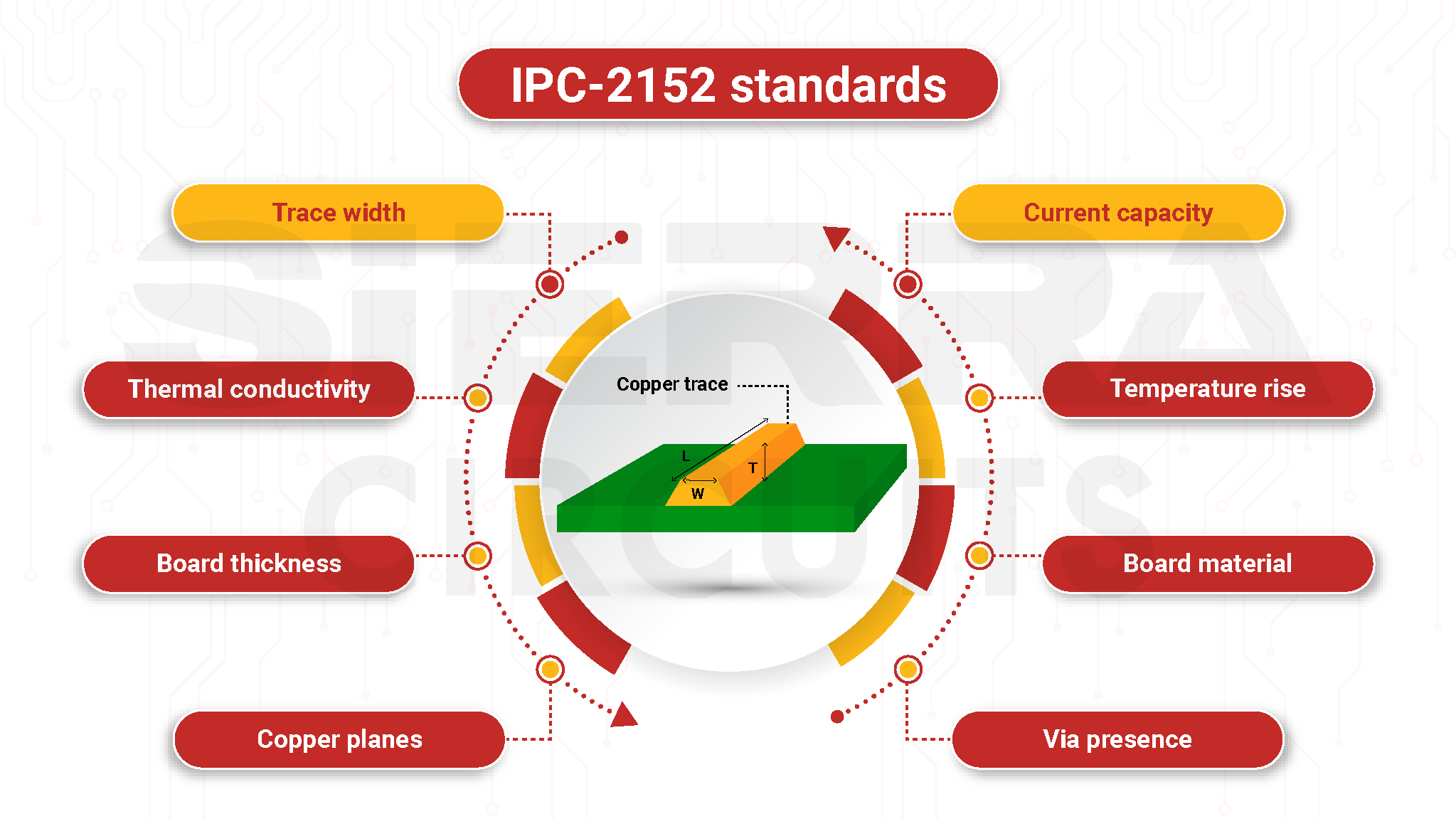
The IPC-2152 standard helps you optimize the current capacity, temperature rise, and width of a trace for efficient thermal management.| Sierra Circuits
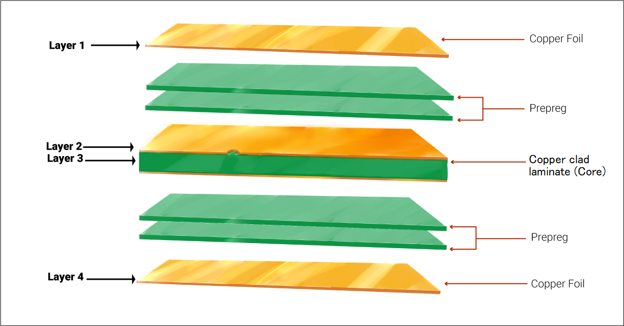
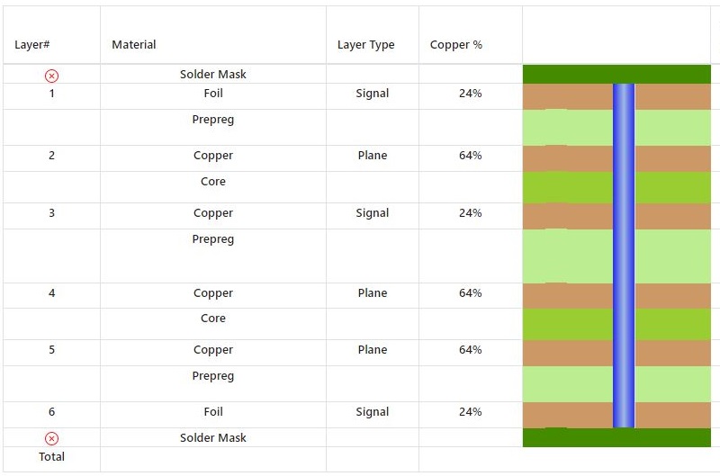
A multilayer PCB has more than two layers in its stack-up. The stack-up describes the construction of a multilayer board in sequential order.| Sierra Circuits
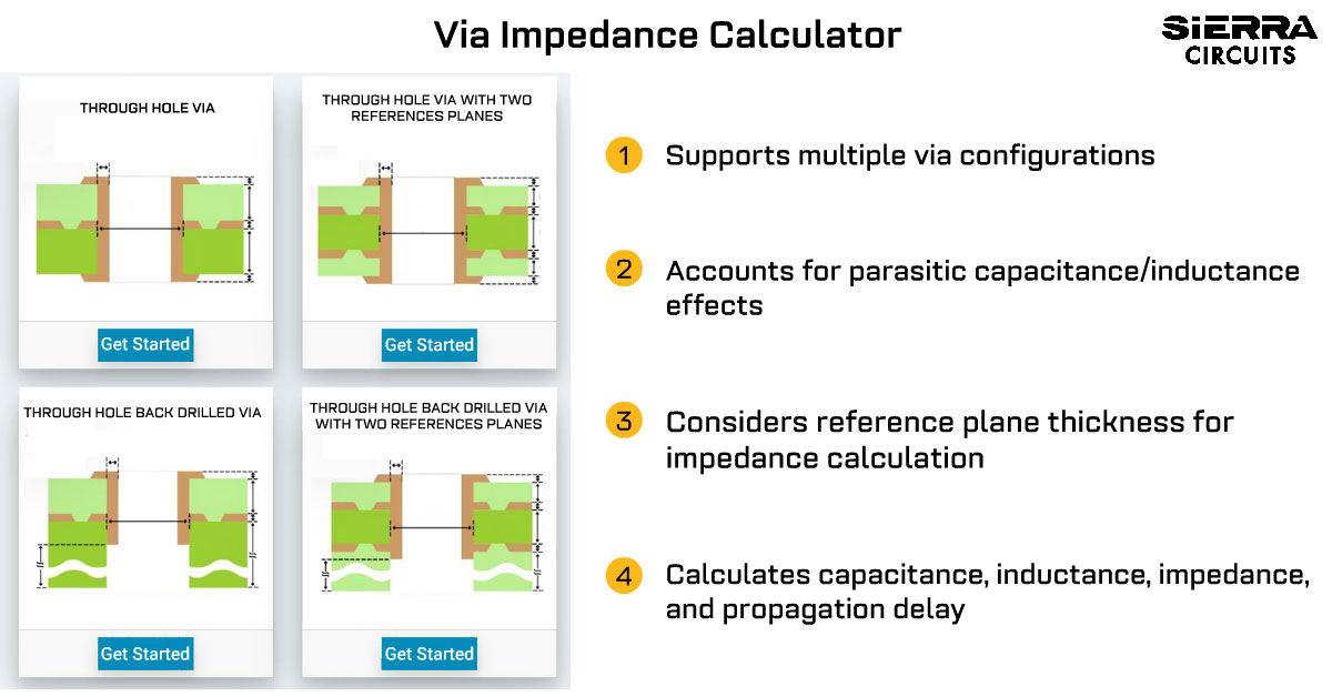
The Impedance Calculator evaluates single-ended and differential impedance, signal losses, and crosstalk for various impedance models.| Sierra Circuits
Sierra Circuits offers quickturn, high-quality, HDI printed circuit boards. Learn about our HDI PCB capabilities.| Sierra Circuits

To build an efficient PCB stack-up, select the right materials, estimate the number of signal layers, and optimally arrange the layers.| Sierra Circuits
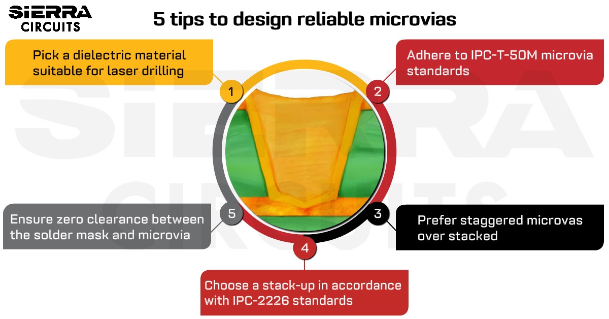
Design strategies for reliable microvias include selecting laser drillable materials and adhering to IPC-T-50M and IPC-2226 standards.| Sierra Circuits
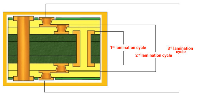
Sequential lamination is a process of fabricating a high-density PCB using cores and subsets composed of copper and dielectric layers.| Sierra Circuits
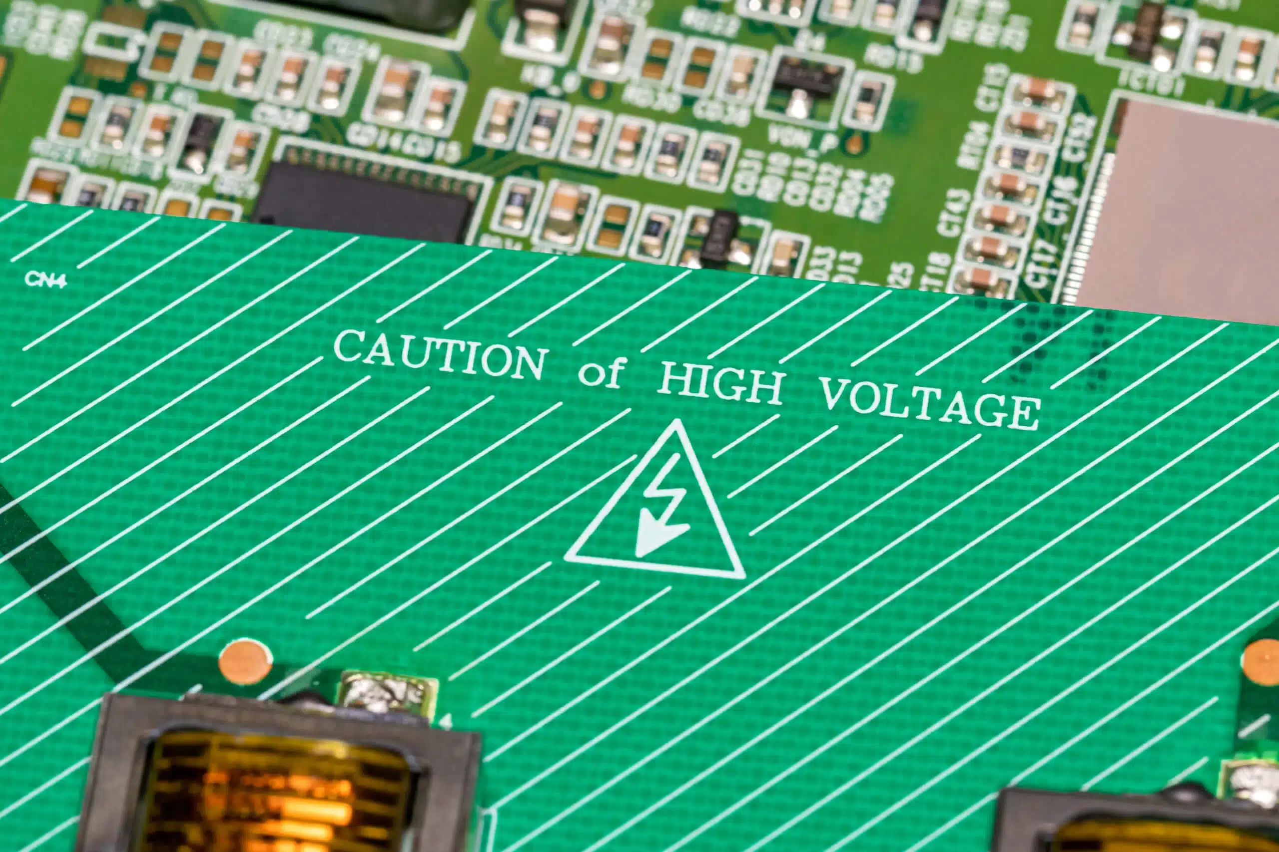
High voltage circuit boards require accurate layout since the traces carry hazardous voltages. Read more now!| Sierra Circuits
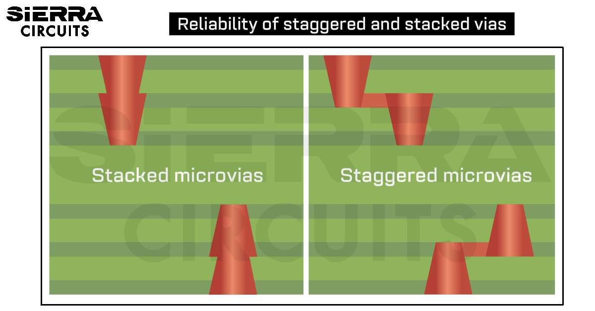
Staggered and stacked vias play crucial role in designing HDI boards. The compact design is highly functional with great signal integrity.| Sierra Circuits
Here are some best high-speed PCB routing practices that will help PCB designers to craft a perfect design.| Sierra Circuits
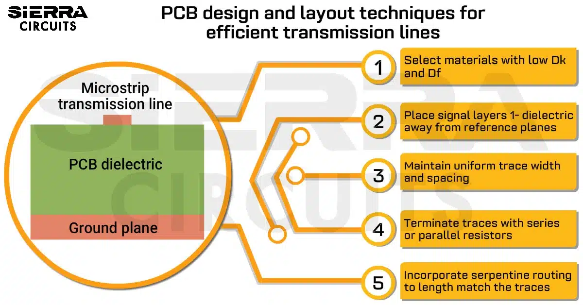
When designing PCB transmission lines, terminate the traces accurately and maintain a uniform trace width and spacing.| Sierra Circuits
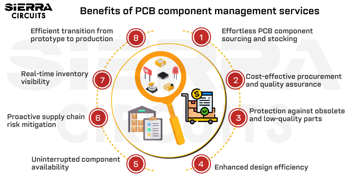
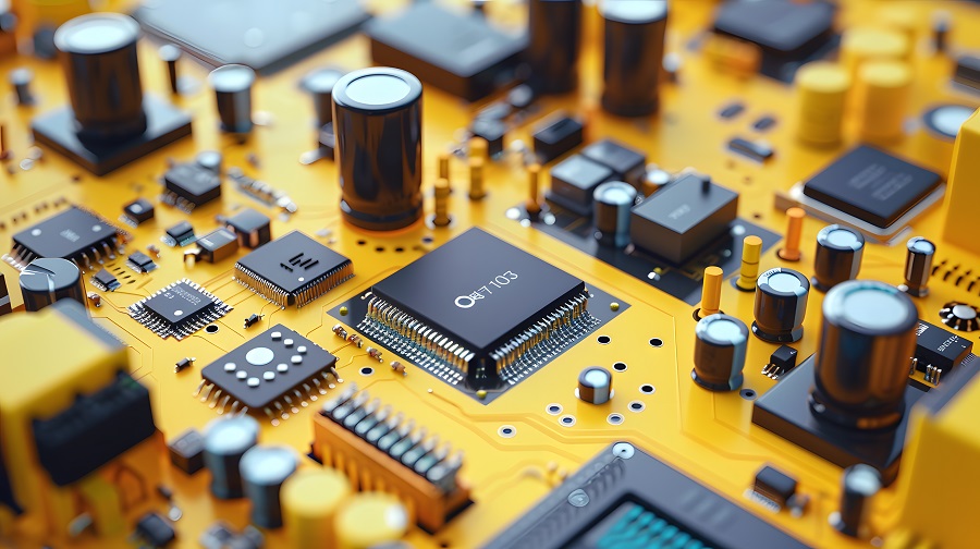
PCB component management services provide supply chain solutions by helping you procure, store, and manage high-quality parts.| Sierra Circuits
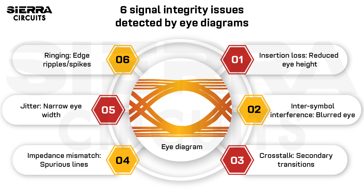
Eye diagrams reveal critical signal integrity issues like Inter-symbol interference, jitter, crosstalk, ringing, and reflections.| Sierra Circuits
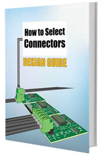
Download the Connector Design Guide which helps you select the right connector and covers terminology, selection and layout rules, and more.| Sierra Circuits
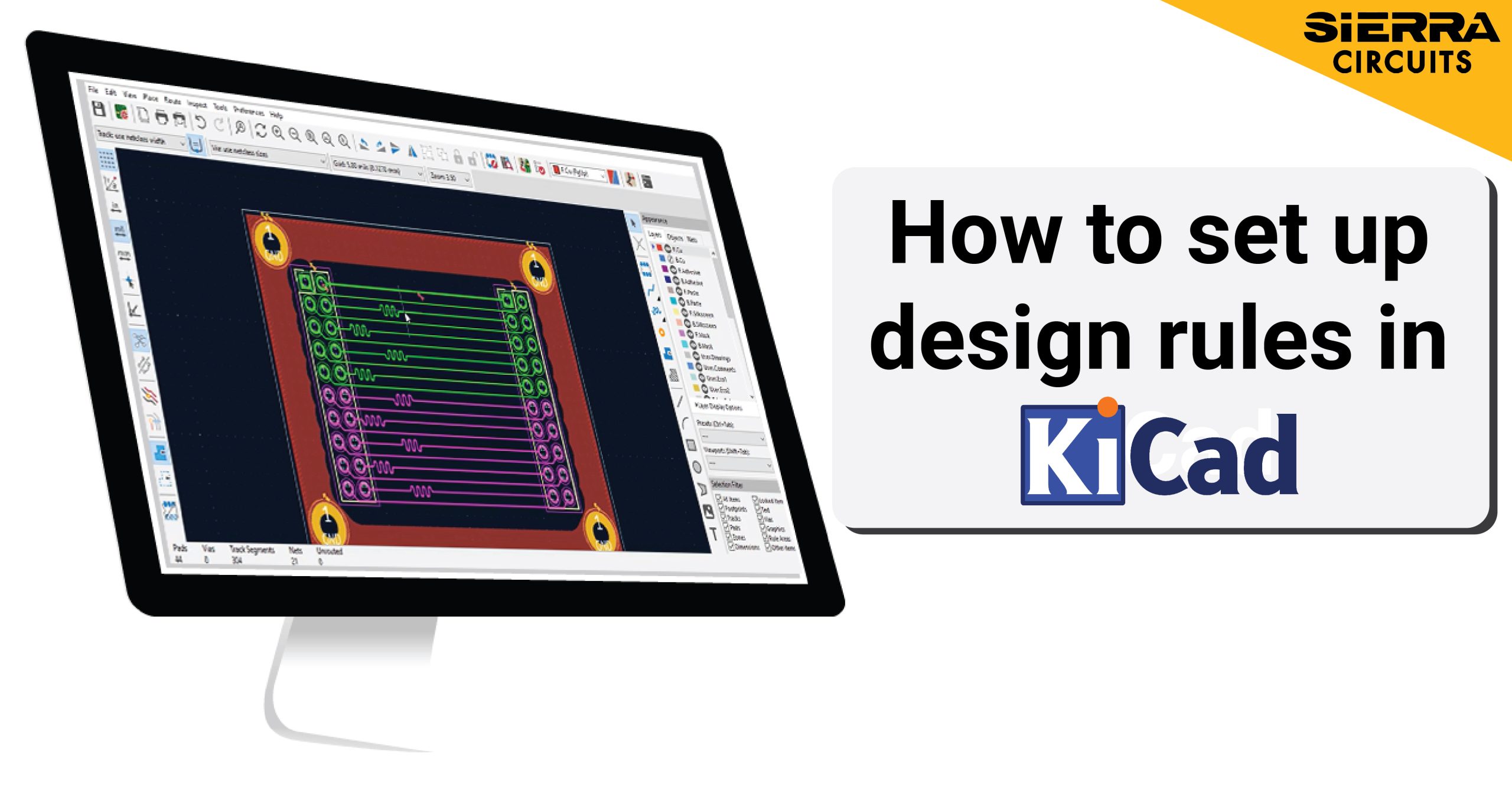
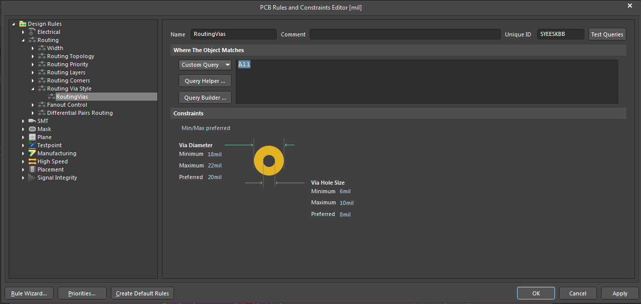
In this tutorial, you'll learn how to set up design rules in KiCad, such as trace width, clearance, via size, and net classes.| Sierra Circuits
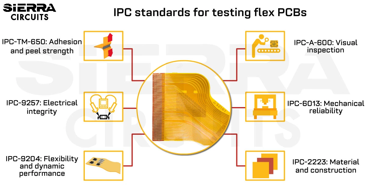
IPC flex PCB testing standards like IPC-2223 and IPC-9204 define how CMs should evaluate the electrical and mechanical reliability of FPCs.| Sierra Circuits
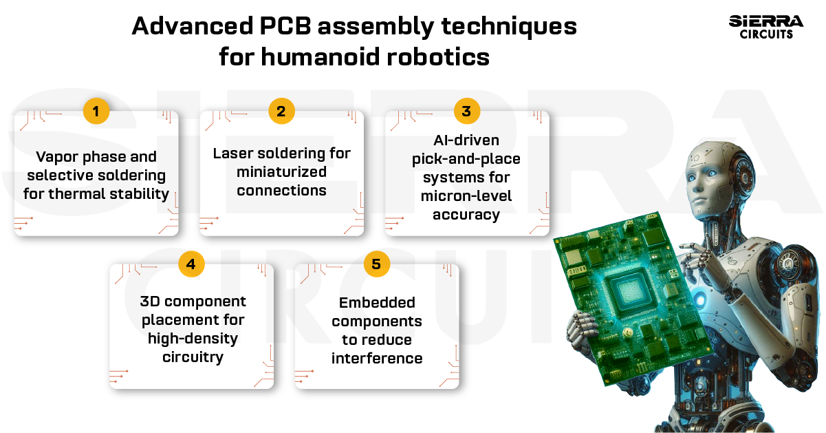
Humanoid robotics PCB assembly requires advanced techniques like AI-driven component placement and 3D circuit integration.| Sierra Circuits
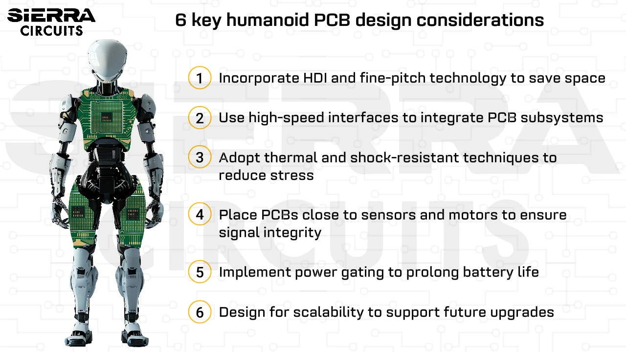
When designing humanoid robotics PCBs, use high-frequency materials and incorporate FPCs to integrate sensors.| Sierra Circuits
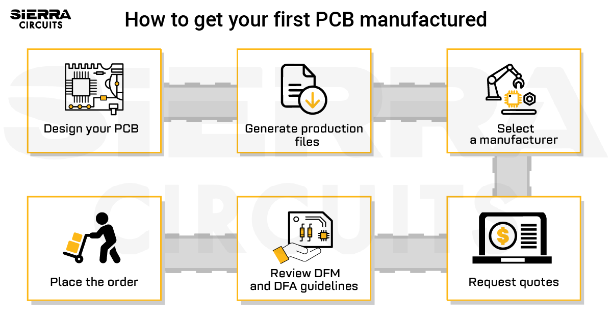
To get your first PCB manufactured, design your board, select a manufacturer, perform DFM and DFA analysis, and place the order.| Sierra Circuits
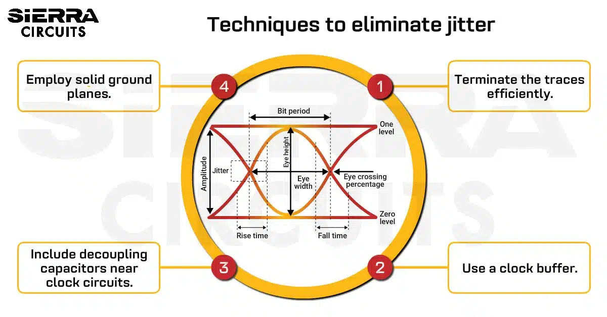
To avoid jitter in PCBs, terminate the traces efficiently and incorporate decoupling capacitors near clock drivers and receivers.| Sierra Circuits
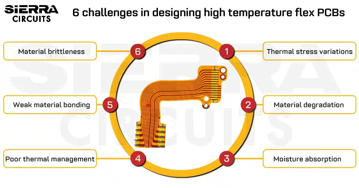
When designing high temperature flex PCBs, consider adhesiveless laminates, use cross-hatched ground planes, and incorporate stiffeners.| Sierra Circuits
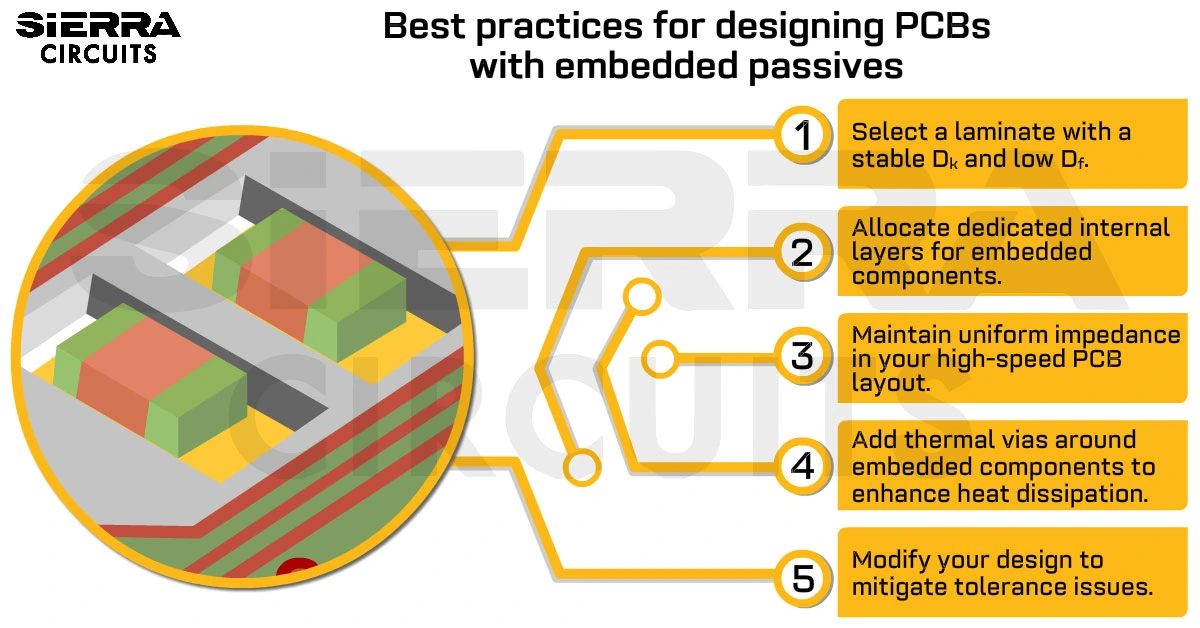
Embedded PCB components are passive devices fabricated within the PCB substrate. They reduce parasitic effects and enhance heat dissipation.| Sierra Circuits
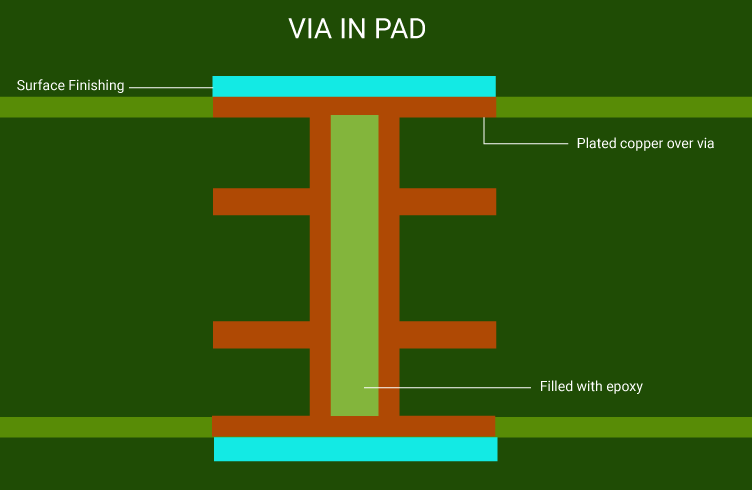
Use via-in-pad technology when the board size is limited, components have small footprints, and surface routing options are restricted.| Sierra Circuits
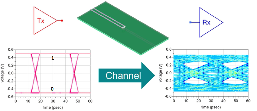
Signal integrity is the measurement of a signal’s quality when it propagates from the transmitter to the receiver in an electronic system.| Sierra Circuits
Drilling is the most expensive and time-consuming process in PCB manufacturing. A small fault in the drilling process leads to a great loss.| Sierra Circuits

PCB via current carrying capacity can be regulated using the process of tenting, plugging, and via current calculators.| Sierra Circuits
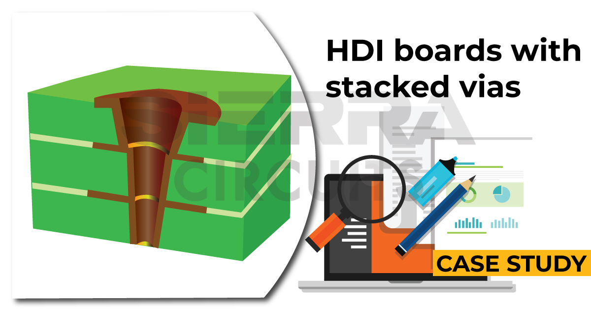
This case study focuses on the challenges and solutions that we implemented to design complex HDI boards with stacked vias.| Sierra Circuits
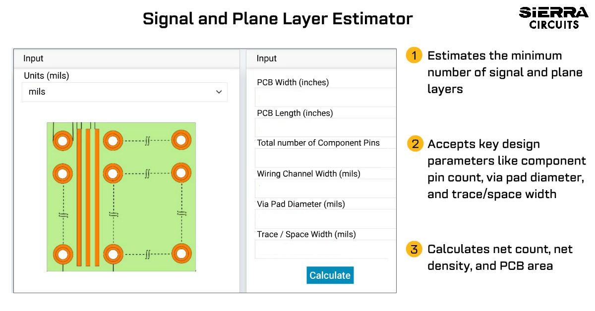
Try this easy-to-use PCB signal and plane layer estimator based on parameters like dimensions, component pin numbers, via pad diameters, etc.| Sierra Circuits
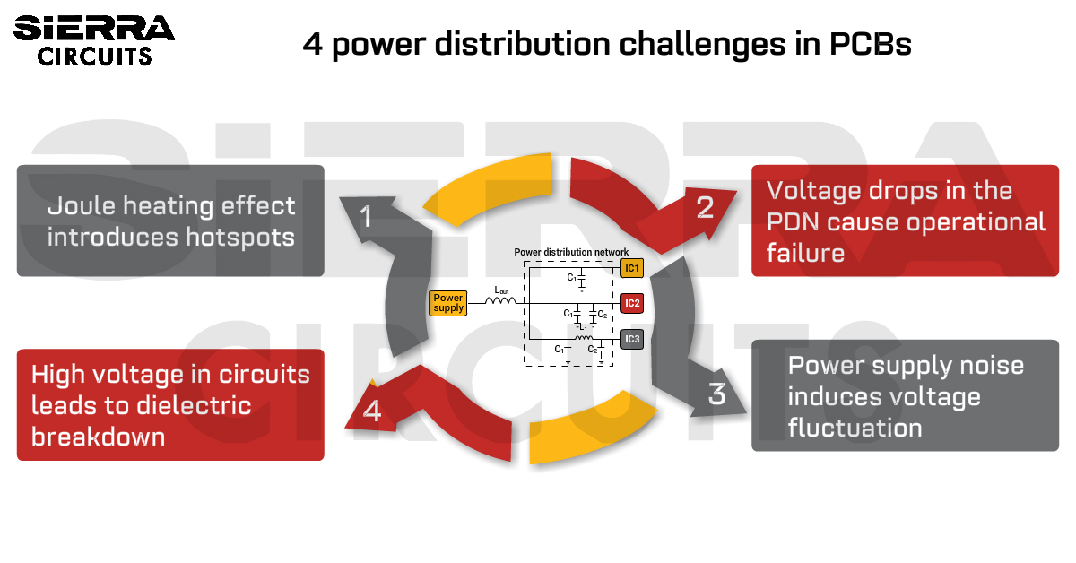
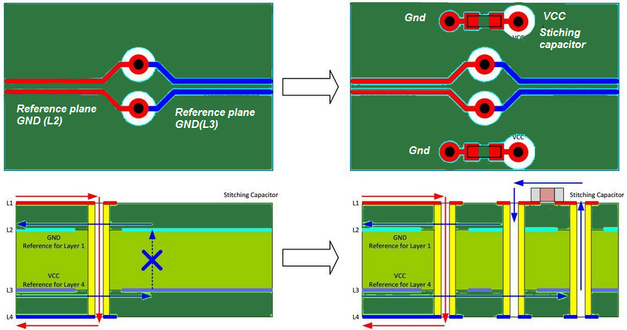
Employ decoupling capacitors, ferrite beads, and Faraday cages to suppress the power supply noise in your PDN design.| Sierra Circuits
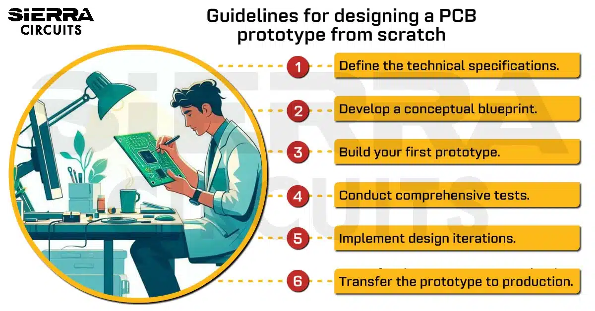
Designing a PCB prototype involves defining specifications, developing the system, testing, iterating, and validating with EVT samples.| Sierra Circuits
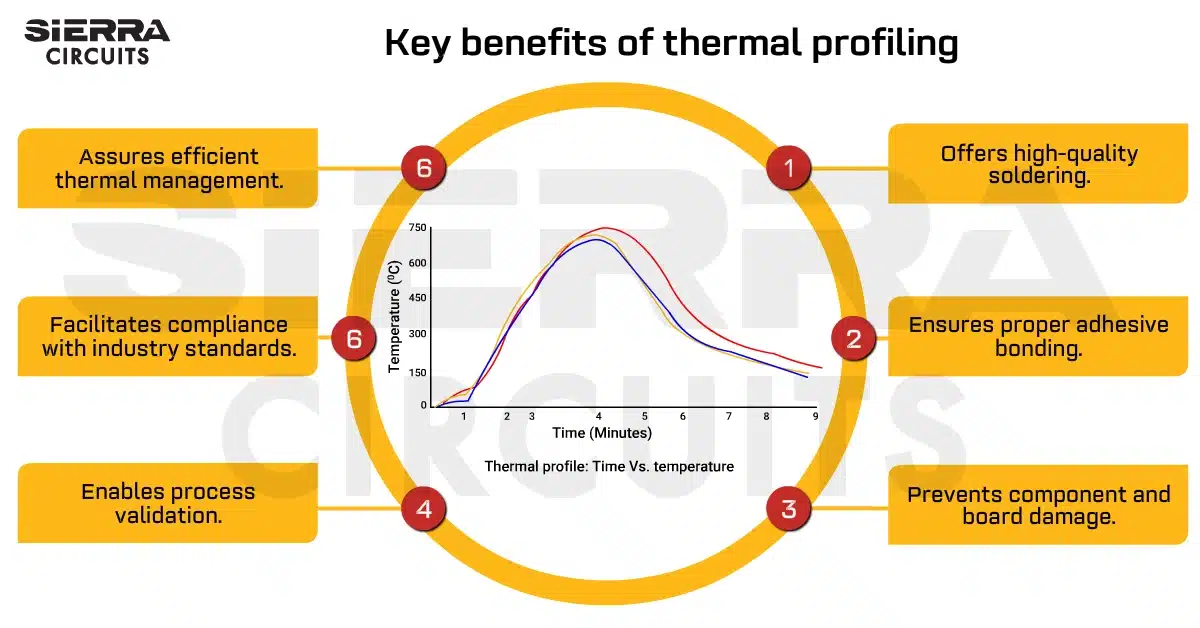
Thermal profiles capture the temperature changes a PCB undergoes during solder reflow or thermal curing, using sensors called thermocouples.| Sierra Circuits
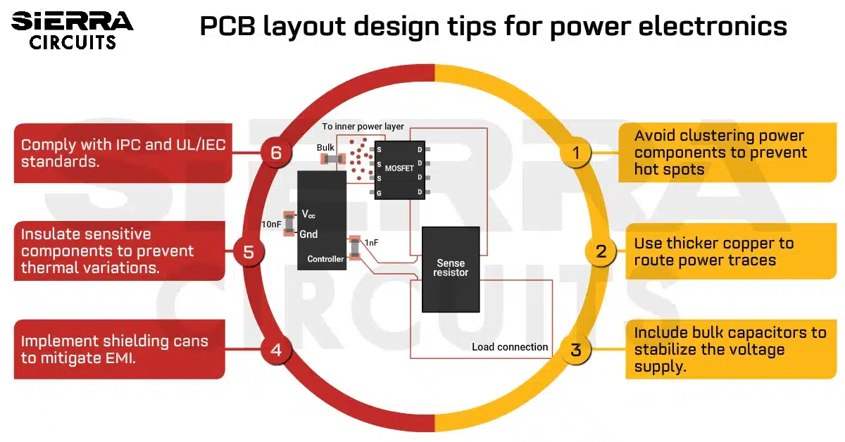
When designing a power electronics PCB, pick high thermal conductivity materials, integrate protection devices, and adhere to IPC standards.| Sierra Circuits
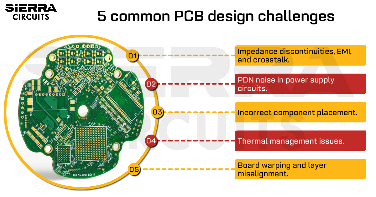
Learn the solutions for 5 common PCB design challenges like impedance discontinuities, EMI, crosstalk, part overlap, and PDN noise.| Sierra Circuits
