Mini-Consortia Forming Around Chiplets
Commercial chiplet marketplaces are still on the distant horizon, but companies are getting an early start with more limited partnerships.| Semiconductor Engineering
Commercial chiplet marketplaces are still on the distant horizon, but companies are getting an early start with more limited partnerships.| Semiconductor Engineering

eBook: Nearly everything you need to know about memory, including detailed explanations of the different types of memory; how and where these are used today; what's changing, which memories are successful and which ones might be in the future; and the limitations of each memory type.| Semiconductor Engineering

In the semiconductor industry, we talk about Moore’s law all the time and yet few understand the history of the so-called law and what it actually says. In this way, it has almost come to represent whatever people want it to show with the general assumption that it predicts future increases in size, complexity or... » read more| Semiconductor Engineering
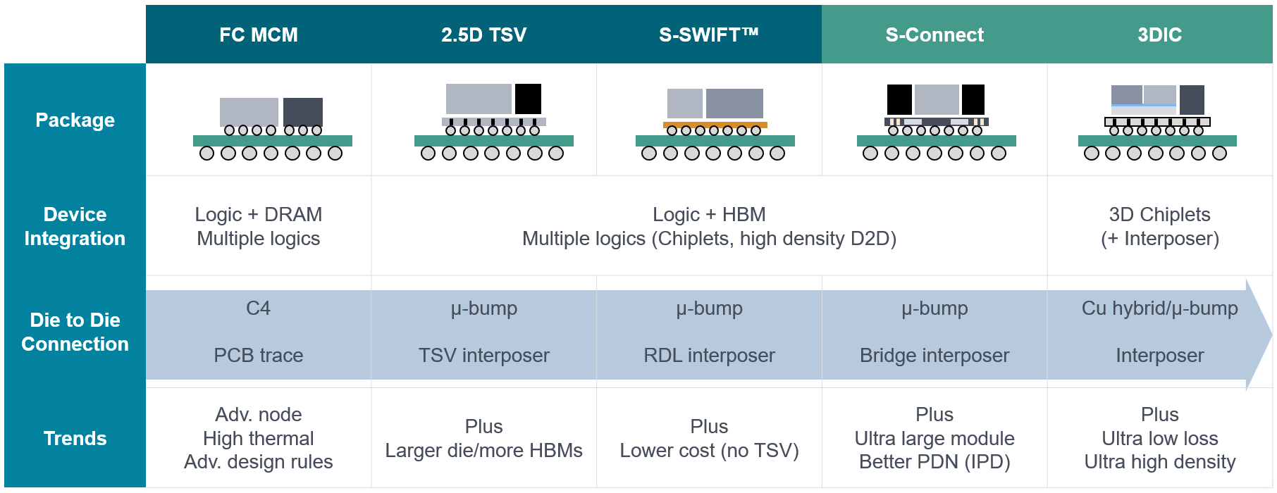
Two or more integrated circuit dies that are stacked on top of each other. The access mechanism connects only to the bottom die. The classic definition that has emerged for 3D ICs is logic on logic, connected with through-silicon vias (TSV). But there are other iterations of this idea, ranging from package-on-package (PoP), homogeneous memory... » read more| Semiconductor Engineering

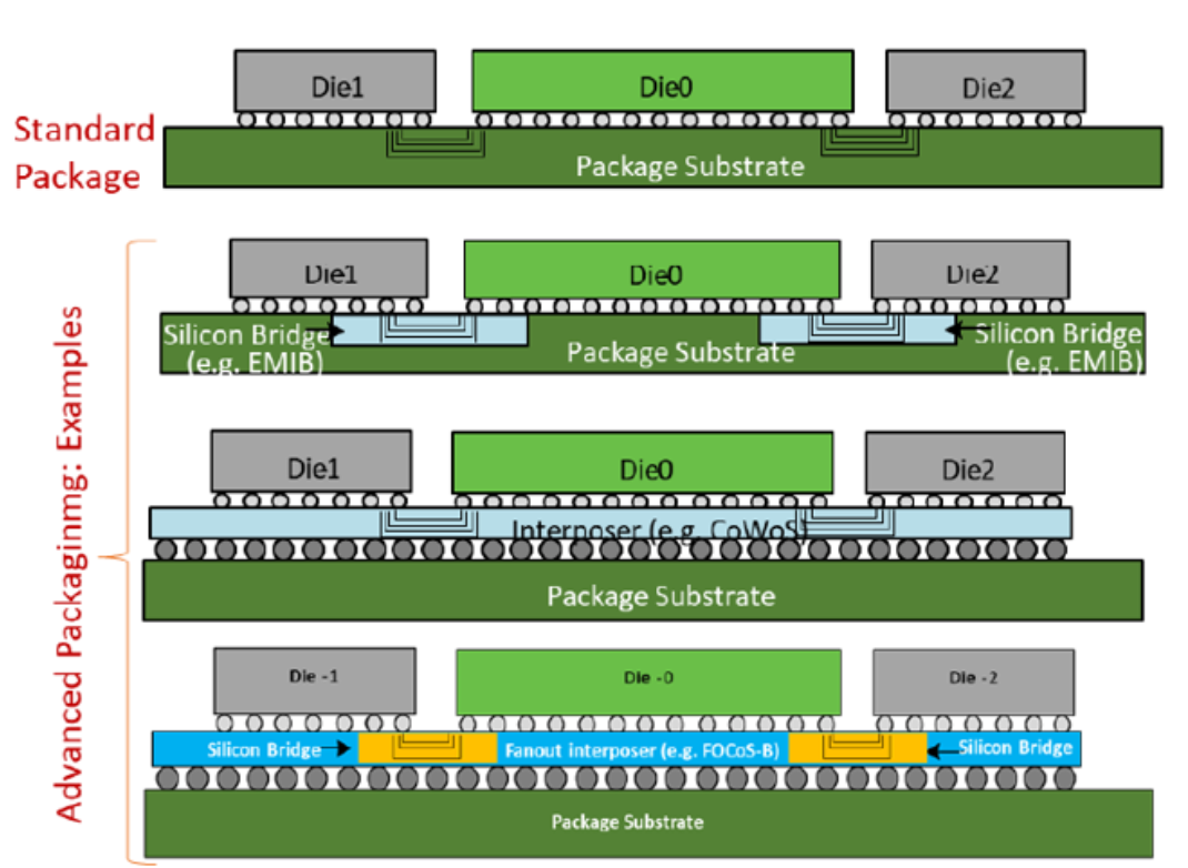
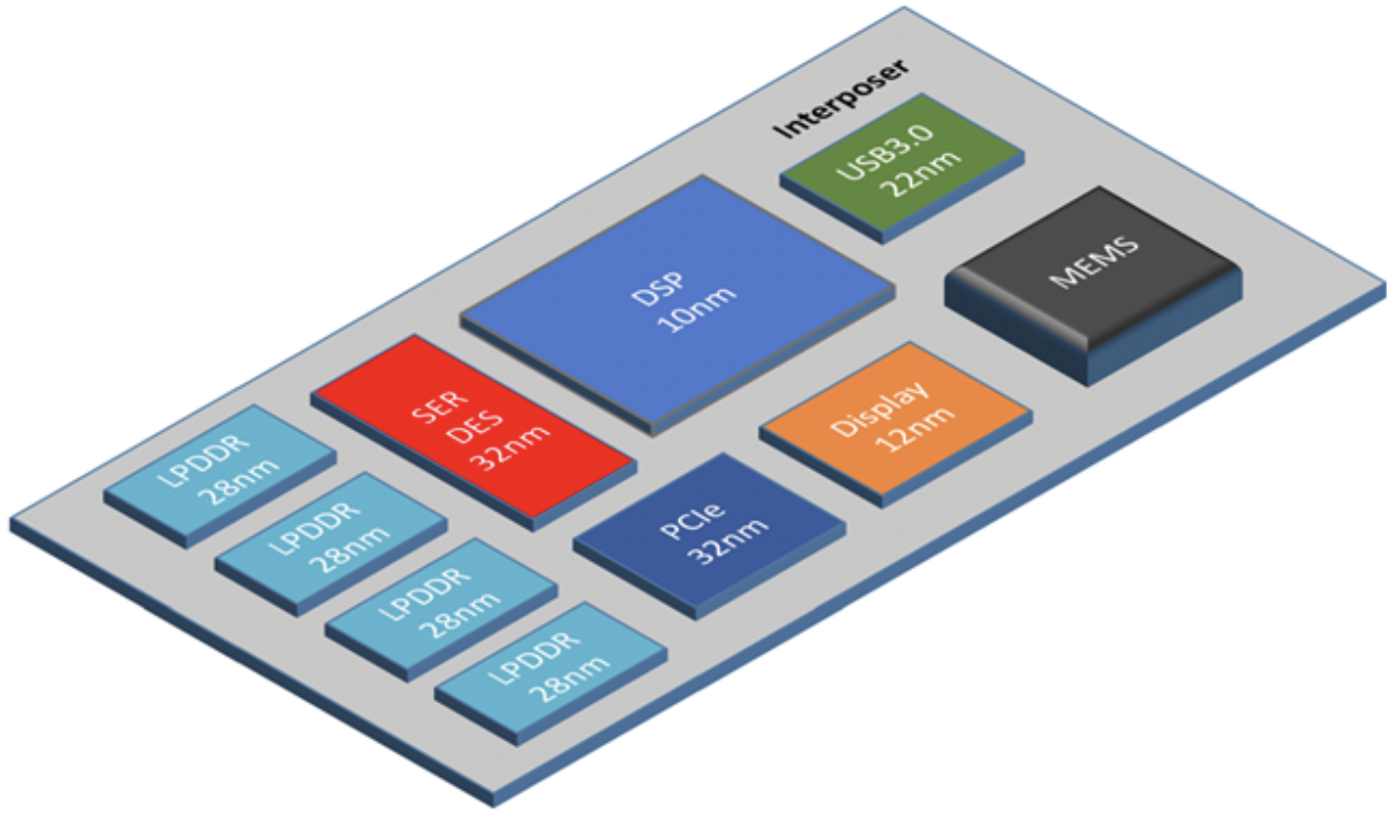
2.5D is a packaging methodology for including multiple die inside the same package The approach typically has been used for applications where performance and low power are critical. Communication between chips is accomplished using either a silicon or organic interposer, typically a chip or layer with through-silicon vias for communication. While communication between chips is... » read more| Semiconductor Engineering
Forksheet FETs are currently in development for 2nm. They fall under the gate-all-around category. In forksheet FETs, both nFET and pFET are integrated in the same structure. A dielectric wall separates the nFET and pFET. This is different from existing gate-all-around FETs, which use different devices for the nFETs and pFETs. Forksheet FETs allow for... » read more| Semiconductor Engineering
Slated for 2.5nm and beyond, complementary FET (CFET) is a more complex version of a gate-all-around device. Traditional gate-all-around FETs stack several p-type wires on top of each other. In a separate device, the transistor stacks n-type wires on each other. In CFETs, the idea is to stack both nFET and pFET wires on each... » read more| Semiconductor Engineering
Universal Chiplet Interconnect Express, or UCIe, is a specification that defines the interconnect between chiplets within a package. Leveraging the PCI Express (PCIe) and Compute Express Link (CXL) standards, UCIe covers the die-to-die I/O physical layer, die-to-die protocols, software stack, and compliance testing. It aims to enable end users to easily mix and match chiplet... » read more| Semiconductor Engineering
Bunch of Wires (BoW) is a chiplet interconnect specification developed by the Open Compute Project Foundation Open Domain-Specific Architecture (ODSA) project. It defines a versatile, open, and interoperable physical interface between two chiplets or chip-scale-packages (CSP) in a common package. The ODSA die-to-die (D2D) communication architecture consists of: A protocol layer that defines communication between... » read more| Semiconductor Engineering
Arm is a developer of a wide variety of IP including processor cores, graphics, and physical IP. One of Arm’s focuses is energy-efficient processor designs. Executive Insight: Simon Segars ARM’s CEO talks about the next five years, the opportunities surrounding the IoT, security, interconnects, and microservers. HQ: Cambridge, UK Known For: IP Other names: Arm... » read more| Semiconductor Engineering
Pros and cons of a middle-ground chiplet assembly that combines 2.5D and 3D-IC.| Semiconductor Engineering
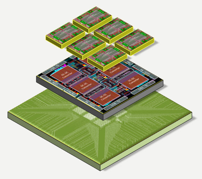
Discrete unpackaged die that can be assembled into a package with other chiplets; each chiplet is optimized to its function.| Semiconductor Engineering
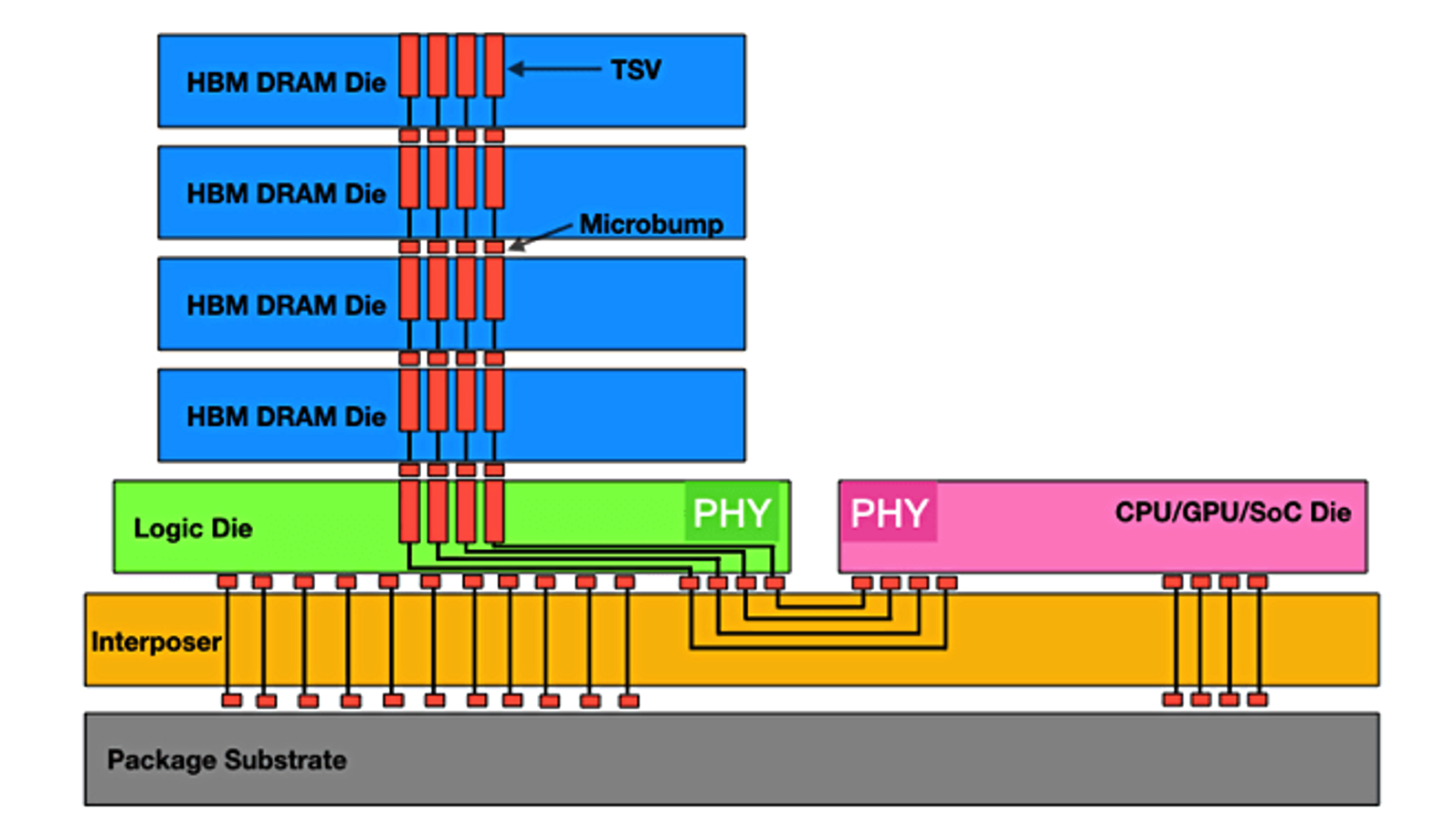
High-bandwidth memory (HBM) is standardized stacked memory technology that provides very wide channels for data, both within the stack and between the memory and logic. An HBM stack can contain up to eight DRAM modules, which are connected by two channels per module. Current implementations include up to four chips, which is roughly the equivalent... » read more| Semiconductor Engineering
