
How Photonics And Handheld Ultrasounds Are Transforming Medical Imaging
AI and capacitive micromachined ultrasonic transducer chips are making diagnostics faster and more accessible.| Semiconductor Engineering
New concerns and challenges for memory in AI data centers. The post Critical Factors For Storing Data In DRAM appeared first on Semiconductor Engineering.| Semiconductor Engineering
A new approach enhances AI understanding through hierarchical clustering techniques with LLM-driven keyphrase extraction. The post Unlocking Clarity: Keyphrase Trees Bring Structure To AI Text Analysis appeared first on Semiconductor Engineering.| Semiconductor Engineering
Designing dummy patterning to achieve optimal etch results. The post Using Virtual Twins To Accelerate The Transition From Layout To Semiconductor Manufacturing appeared first on Semiconductor Engineering.| Semiconductor Engineering
The state of photomask revenues, EUV pellicles, and curvilinear masks. The post Expert Panel Sees History Of Continuous Photomask Innovations As Key To The Future appeared first on Semiconductor Engineering.| Semiconductor Engineering
AI and capacitive micromachined ultrasonic transducer chips are making diagnostics faster and more accessible.| Semiconductor Engineering
U.S.-China countermoves; Nexperia fallout; ASE's acquisition; SEMI's cyber tool + 90,000 job openings; 3D-IC design; data center forecast; agentic AI funding; Intel, Lam, ST, TI earnings; Applied Materials layoffs; India's 7nm; Pakistan's initiative. The post Chip Industry Week in Review appeared first on Semiconductor Engineering.| Semiconductor Engineering
Modeling, simulation, and digital twins enable EUV innovation. The post Charting The Frontiers Of Photomask Technology And Extreme Ultraviolet Lithography appeared first on Semiconductor Engineering.| Semiconductor Engineering
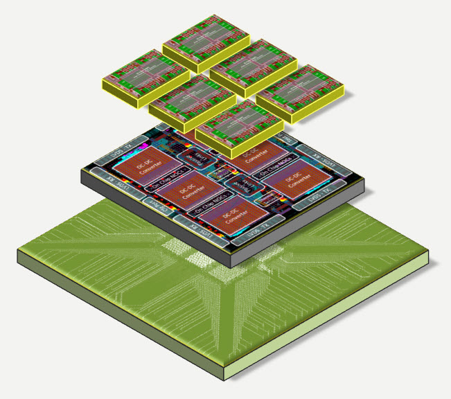
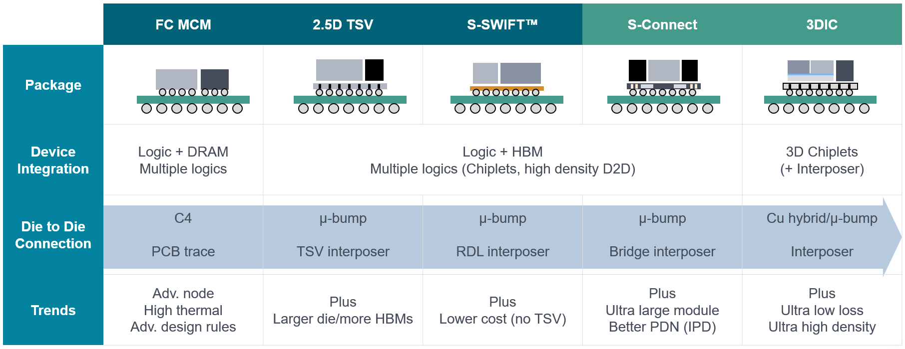
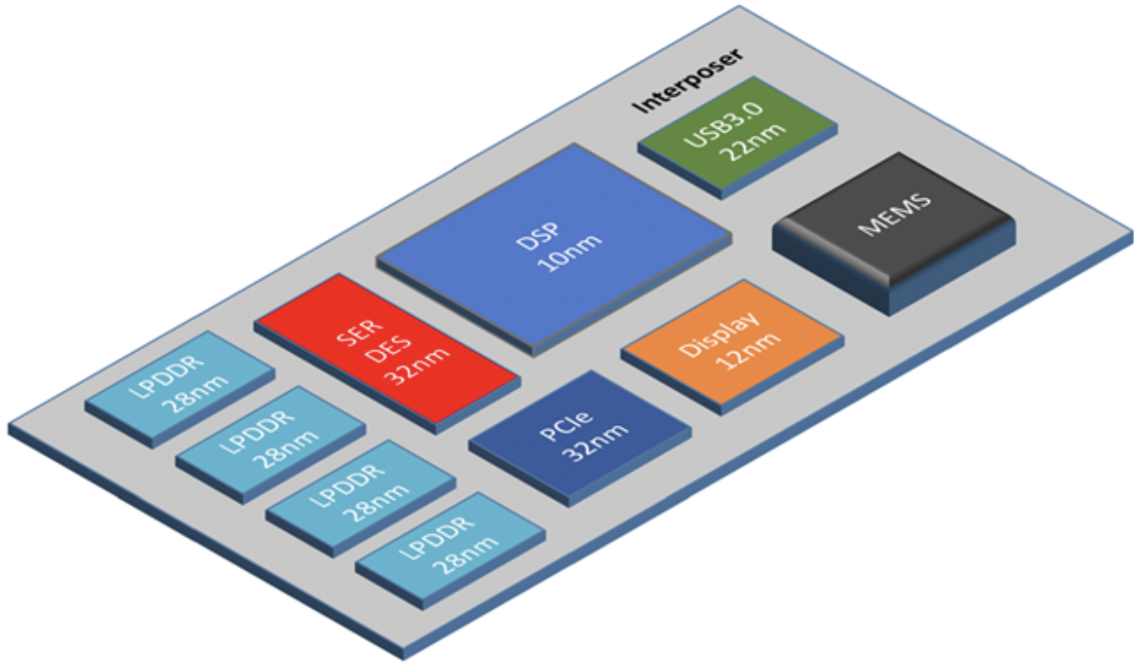
Advanced packaging will be key to unlocking performance, efficiency, and innovation across the data spectrum. The post Enabling The Future: Heterogeneous Integration From Connected Devices To Data Centers appeared first on Semiconductor Engineering.| Semiconductor Engineering
Packaging moves toward predictive control, but trust and validation still lag. The post Digital Twins For Packaging: Bridging Design, Fab, Test, And Reliability appeared first on Semiconductor Engineering.| Semiconductor Engineering
Smarter manufacturing of smarter chips dominated the agenda at this year's SEMICON West. The post Powering Efficiency: AI Transforms IC Manufacturing As ICs Fuel AI appeared first on Semiconductor Engineering.| Semiconductor Engineering

A new technical paper titled “Three-dimensional integrated hybrid complementary circuits for large-area electronics” was published by researchers at KAUST, Imperial College London and the University of Manchester. Abstract “The development of low-power computing sectors requires compact, power-efficient and high-performance integrated circuits. Hybrid technology that combines n-type metal oxide thin-film transistors and p-type organic thin-film transistors... » read more| Semiconductor Engineering

2D semiconductors: Direct patterning with UV; gate stack roadmap; flash memory integration.| Semiconductor Engineering

A new technical paper titled “ShuffleV: A Microarchitectural Defense Strategy against Electromagnetic Side-Channel Attacks in Microprocessors” was published by researchers at Northeastern University and Binghamton University. Abstract “The run-time electromagnetic (EM) emanation of microprocessors presents a side-channel that leaks the confidentiality of the applications running on them. Many recent works have demonstrated successful attacks leveraging... » read more| Semiconductor Engineering
Chiplets may be the semiconductor industry’s hardest challenge yet, but they are the best path forward.| Semiconductor Engineering

Assembling systems from physical IP is gaining mindshare, but there are technical, business and logistical issues that need to be resolved before this will work.| Semiconductor Engineering

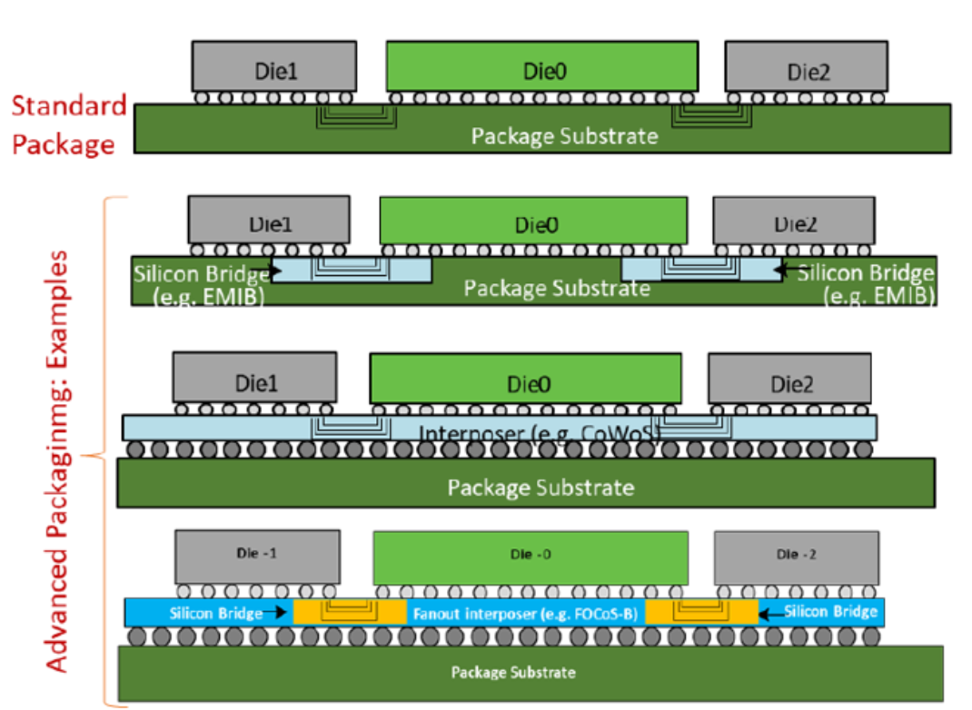
A system in package, or SiP, is a way of bundling two or more ICs inside a single package. This is in contrast to a system on chip, or SoC, where the functions on those chips are integrated onto the same die. SiP has been around since the 1980s in the form of multi-chip modules.... » read more| Semiconductor Engineering
Integrating different chips, chiplets, and components into a single package.| Semiconductor Engineering
A system-on-chip (SoC) is the integration of functions necessary to implement an electronic system onto a single substrate and contains at least one processor. The only real difference between an SoC and a microcontroller is one of scale. The integration of multiple blocks onto a single substrate has multiple advantages including cost and lower power... » read more| Semiconductor Engineering

Packaging is an essential part of semiconductor manufacturing and design. It affects power, performance, and cost on a macro level, and the basic functionality of all chips on a micro level. The package is the container that holds the semiconductor die. The packaging may be done by a separate vendor, the OSAT, although foundries are... » read more| Semiconductor Engineering

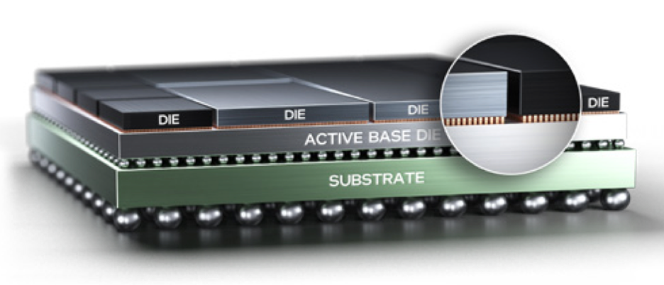
Advanced packaging is a general grouping of a variety of distinct techniques, including 2.5D, 3D-IC, fan-out wafer-level packaging and system-in-package. While putting multiple chips in a package has been around for decades, the driver for advanced packaging is directly correlated with Moore’s Law. Wires are shrinking along with transistors, and the amount of distance that... » read more| Semiconductor Engineering
Extreme ultraviolet (EUV) lithography is a soft X-ray technology, which has a wavelength of 13.5nm. Today’s EUV scanners enable resolutions down to 22nm half-pitch. In a system, an EUV light source makes use of a high power laser to create a plasma. This, in turn, helps emit a short wavelength light inside a vacuum chamber.... » read more| Semiconductor Engineering
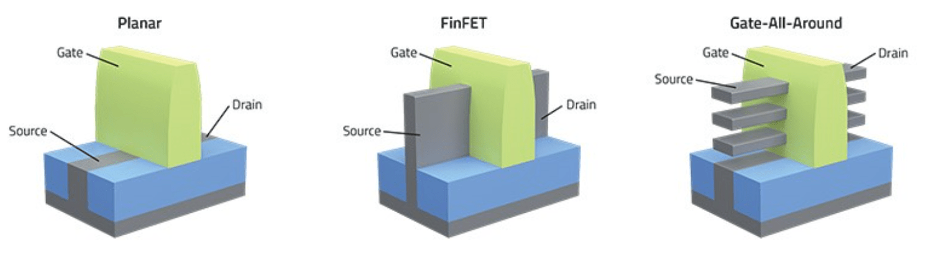
Gate-all-around FET (GAA FET) is a modified transistor structure where the gate contacts the channel from all sides. It’s basically a silicon nanowire with a gate going around it. In some cases, the gate-all-around FET could have InGaAs or other III-V materials in the channels. Introduced by major foundries around the 3nm/2nm nodes when further scaling... » read more| Semiconductor Engineering
A field programmable gate array (FPGA) is a semiconductor device than can take on the personality of a customer’s design by programming it. Unlike a processor that executes a program, and FPGA configures itself to become an operating circuit that will then respond to inputs in the same way that a dedicated piece of hardware... » read more| Semiconductor Engineering

Five process nodes in four years, high-NA EUV, 3D-ICs, chiplets, hybrid bonding, and more.| Semiconductor Engineering
This website uses cookies to improve your experience while you navigate through the website. The cookies that are categorized as necessary are stored on your browser as they are essential for the working of basic functionalities of the website. We also use third-party cookies that help us analyze and understand how you use this website. We do not sell any personal information.| Semiconductor Engineering
Commercial chiplet marketplaces are still on the distant horizon, but companies are getting an early start with more limited partnerships.| Semiconductor Engineering

eBook: Nearly everything you need to know about memory, including detailed explanations of the different types of memory; how and where these are used today; what's changing, which memories are successful and which ones might be in the future; and the limitations of each memory type.| Semiconductor Engineering
In the semiconductor industry, we talk about Moore’s law all the time and yet few understand the history of the so-called law and what it actually says. In this way, it has almost come to represent whatever people want it to show with the general assumption that it predicts future increases in size, complexity or... » read more| Semiconductor Engineering
Two or more integrated circuit dies that are stacked on top of each other. The access mechanism connects only to the bottom die. The classic definition that has emerged for 3D ICs is logic on logic, connected with through-silicon vias (TSV). But there are other iterations of this idea, ranging from package-on-package (PoP), homogeneous memory... » read more| Semiconductor Engineering

2.5D is a packaging methodology for including multiple die inside the same package The approach typically has been used for applications where performance and low power are critical. Communication between chips is accomplished using either a silicon or organic interposer, typically a chip or layer with through-silicon vias for communication. While communication between chips is... » read more| Semiconductor Engineering
Forksheet FETs are currently in development for 2nm. They fall under the gate-all-around category. In forksheet FETs, both nFET and pFET are integrated in the same structure. A dielectric wall separates the nFET and pFET. This is different from existing gate-all-around FETs, which use different devices for the nFETs and pFETs. Forksheet FETs allow for... » read more| Semiconductor Engineering
Slated for 2.5nm and beyond, complementary FET (CFET) is a more complex version of a gate-all-around device. Traditional gate-all-around FETs stack several p-type wires on top of each other. In a separate device, the transistor stacks n-type wires on each other. In CFETs, the idea is to stack both nFET and pFET wires on each... » read more| Semiconductor Engineering
Universal Chiplet Interconnect Express, or UCIe, is a specification that defines the interconnect between chiplets within a package. Leveraging the PCI Express (PCIe) and Compute Express Link (CXL) standards, UCIe covers the die-to-die I/O physical layer, die-to-die protocols, software stack, and compliance testing. It aims to enable end users to easily mix and match chiplet... » read more| Semiconductor Engineering
Bunch of Wires (BoW) is a chiplet interconnect specification developed by the Open Compute Project Foundation Open Domain-Specific Architecture (ODSA) project. It defines a versatile, open, and interoperable physical interface between two chiplets or chip-scale-packages (CSP) in a common package. The ODSA die-to-die (D2D) communication architecture consists of: A protocol layer that defines communication between... » read more| Semiconductor Engineering
Arm is a developer of a wide variety of IP including processor cores, graphics, and physical IP. One of Arm’s focuses is energy-efficient processor designs. Executive Insight: Simon Segars ARM’s CEO talks about the next five years, the opportunities surrounding the IoT, security, interconnects, and microservers. HQ: Cambridge, UK Known For: IP Other names: Arm... » read more| Semiconductor Engineering

GenAI value is creating a huge TAM and revenues are ramping at historically fast rates.| Semiconductor Engineering

As inference proliferates to edge servers and endpoints, memory solutions must balance performance, cost, and power efficiency.| Semiconductor Engineering
Deep insights into the increasingly complex task of designing, testing, integrating, and manufacturing semiconductors. Explore the latest in Semiengineering and cutting-edge chip technology.| Semiconductor Engineering

Tradeoff between precision and speed becomes more critical at advanced nodes.| Semiconductor Engineering

By profiling systems early, designers can address fundamental issues in data flow and resource coordination.| Semiconductor Engineering

How AI is reshaping EDA, and how it will help chipmakers to focus on domain-specific solutions.| Semiconductor Engineering

Broad-line supplier of EDA, IP and software testing tools.| Semiconductor Engineering
Mentor, a Siemens Business, is a broad line EDA supplier. It provides a complete semiconductor design flow that includes simulation, emulation, place and route, verification, design for manufacturing, and test. It also develops tools for wire harness systems and computational fluid dynamics.| Semiconductor Engineering
A full line EDA supplier| Semiconductor Engineering
Baya Systems offers a software-defined, unified fabric for SoCs and chiplets that provides a common transport with support for multiple protocols and coherency needs within a unified design flow. Baya Systems’ NoC is topology-agnostic, and its software enables continuous refinement of data-driven architecture and micro-architecture development from initial specification through post-silicon tuning, with built-in simulation... » read more| Semiconductor Engineering
ChipAgents develops AI agents for EDA workflows to boost RTL design, debugging, and verification productivity. Its ChipAgents AI chip design environment enables designers to transform concepts into precise design specifications using simple language prompts, analyzes and generates RTL design specs and code, auto-completes Verilog, automates the creation of testbenches, and autonomously verifies and debugs design... » read more| Semiconductor Engineering

Why and where limitations are needed in AI-driven design, and where software-defined hardware works best.| Semiconductor Engineering

Narrowly defined verticals offer the best opportunities for AI. Plus, what will the impact be on junior engineers?| Semiconductor Engineering

A small crack early in the fabrication process has the potential to grow into a killer defect later.| Semiconductor Engineering

Measuring how injected faults propagate through a design and how long they remain in the system.| Semiconductor Engineering

Brewer Science develops materials and processes for semiconductor, including anti-reflective coatings to control light during photolithography, materials for packaging chips, protective coating, bonding/debonding materials for fan-out wafer-level packaging, and carbon-based sensors.| Semiconductor Engineering

Keysight Technologies is a test and measurement equipment company. It develops advanced design and validation solutions that span the development lifecycle, including design simulation, prototype validation, automated software testing, manufacturing analysis and network performance optimization and visibility in enterprise, service provider and cloud environments. Customers span worldwide communications and industrial ecosystems, aerospace and defense, automotive,... » read more| Semiconductor Engineering
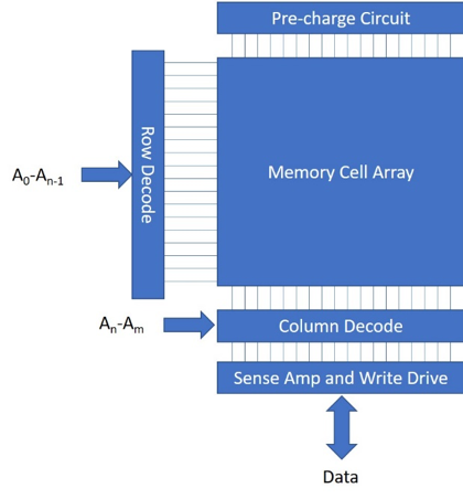
SRAM uses bistable latching circuitry to store each bit. While no refresh is necessary it is still volatile in the sense that data is lost when the memory is not powered. A typical SRAM uses 6 MOSFETs to store each memory bit although additional transistors may become necessary at smaller nodes. Fig 1. Simplified block... » read more| Semiconductor Engineering
ANSYS develops specialized system-level simulation technology for a variety of industries.| Semiconductor Engineering
Pros and cons of a middle-ground chiplet assembly that combines 2.5D and 3D-IC.| Semiconductor Engineering

AI and robotics are taking on bigger, more complex, and increasingly autonomous tasks, but integration with existing equipment and processes remains a formidable challenge.| Semiconductor Engineering

Universities, companies, and governments are forming broad partnerships to update skills and foster innovation in chips, security, AI, and related fields.| Semiconductor Engineering
Discrete unpackaged die that can be assembled into a package with other chiplets; each chiplet is optimized to its function.| Semiconductor Engineering
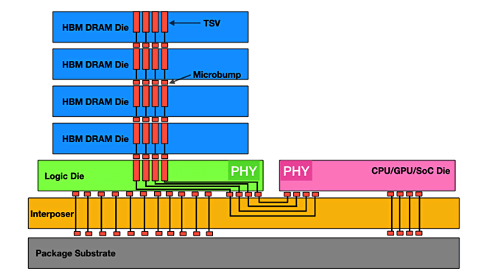
High-bandwidth memory (HBM) is standardized stacked memory technology that provides very wide channels for data, both within the stack and between the memory and logic. An HBM stack can contain up to eight DRAM modules, which are connected by two channels per module. Current implementations include up to four chips, which is roughly the equivalent... » read more| Semiconductor Engineering

Published 8/23/2021 (by Mark LaPedus & Ed Sperling). “Inside Intel’s Ambitious Roadmap” article link is here. Ann Kelleher, senior vice president and general manager of Technology Development at Intel, sat down with Semiconductor Engineering to talk about the company’s new logic roadmap, as well as lithography, packaging, and process technology. What follows are excerpts of... » read more| Semiconductor Engineering
Foundry competition heats up in three dimensions and with novel technologies as planar scaling benefits diminish.| Semiconductor Engineering
