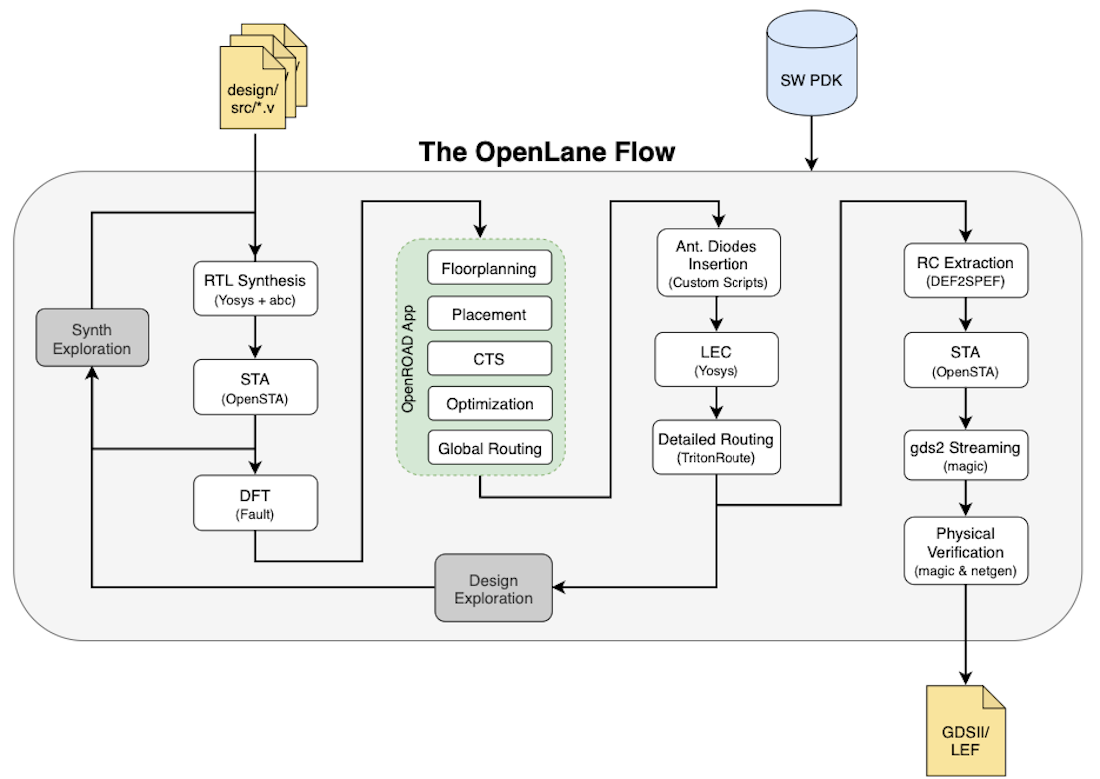
LibreLane is an Open Source ASIC tool. You can download it from here. LibreLane is the new name for OpenLane. After Efabless shutdown the project was transferred to the FOSSi Foundation. OpenLane was released in 2021 and you can watch Mohamed Shalan’s OpenLane FOSSI dialup presentation to find out more about it. Here’s the overview: We put our HDL in at one end, and out the other comes the GDS2 files that are the standard file format for the foundry.| Zero to ASIC Course
Very Large Scale Integration - this term started getting used in the 70s when thousands of MOSFETs were integrated together to make one IC. Image from https://www.computerhistory.org/ Some notable dates: WhatWhoWhen First transistorMorris Tanenbaum1954 First ICKilby & Noyce1958 First MOSFETMohamed M. Atalla & Dawon Kahng1959 CMOS inventedFrank Wanlass1963 Intel 4004, 2300 transistorsFederico Faggin1971 6502 CPU with 3510 transistorsMOS technolog y1975 Z80 CPU with 8500 transistorsFederico Fag...| Terminology on Zero to ASIC Course
Verification covers all areas of checking that a design, at some stage in the design process, is correct. This includes simulation, STA, DRC, LVS, LEC and other checks that are performed. In essence, any step that looks at the design, compares it with some other quantity, and does not alter the design, is part of verification. Simulation offers us a way of checking the design is doing what we expect functionally, but that is almost exactly why simulation on its own isn’t enough. When we sim...| Terminology on Zero to ASIC Course
Layout vs Schematic (or LVS) is an important verification step. After the design has been finished and we have the GDS2 files that we can send to the foundry, we want to check that the design is the same as the input that was described by the HDL or schematic. In the OpenLane tool, at the end we have the LVS step. The netlist is extracted using Magic A tool called Netgen can compare this extracted netlist with the one we get after the synthesis step.| Terminology on Zero to ASIC Course
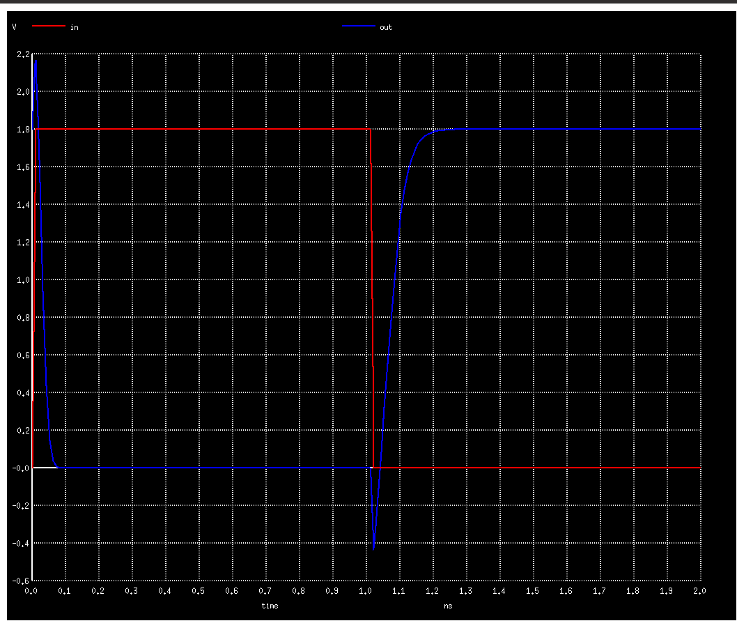
Static Timing Analysis (STA) checks that the design has no setup and hold violations. This is very important, and a failure here could cost you a respin of your ASIC. It is a way of verifying timing quickly without the complexity and time taken to find such issues using back-annotated digital (or even analogue) simulations. Setup violations imply that the circuit runs too slowly to work at the given clock rate, hold violations imply the circuit will fail at any clock speed.| Terminology on Zero to ASIC Course
From Wikipedia: A photomask is an opaque plate with holes or transparencies that allow light to shine through in a defined pattern. They are commonly used in photolithography and the production of integrated circuits (ICs or “chips”) in particular. Masks are used to produce a pattern on a substrate, normally a thin slice of silicon known as a wafer in the case of chip manufacturing. Several masks are used in turn, each one reproducing a layer of the completed design, and together they are...| Terminology on Zero to ASIC Course
From its homepage: Magic is a venerable VLSI layout tool, written in the 1980’s at Berkeley by John Ousterhout, now famous primarily for writing the scripting interpreter language Tcl. Due largely in part to its liberal Berkeley open-source license, magic has remained popular with universities and small companies. The open-source license has allowed VLSI engineers with a bent toward programming to implement clever ideas and help magic stay abreast of fabrication technology. However, it is t...| Terminology on Zero to ASIC Course
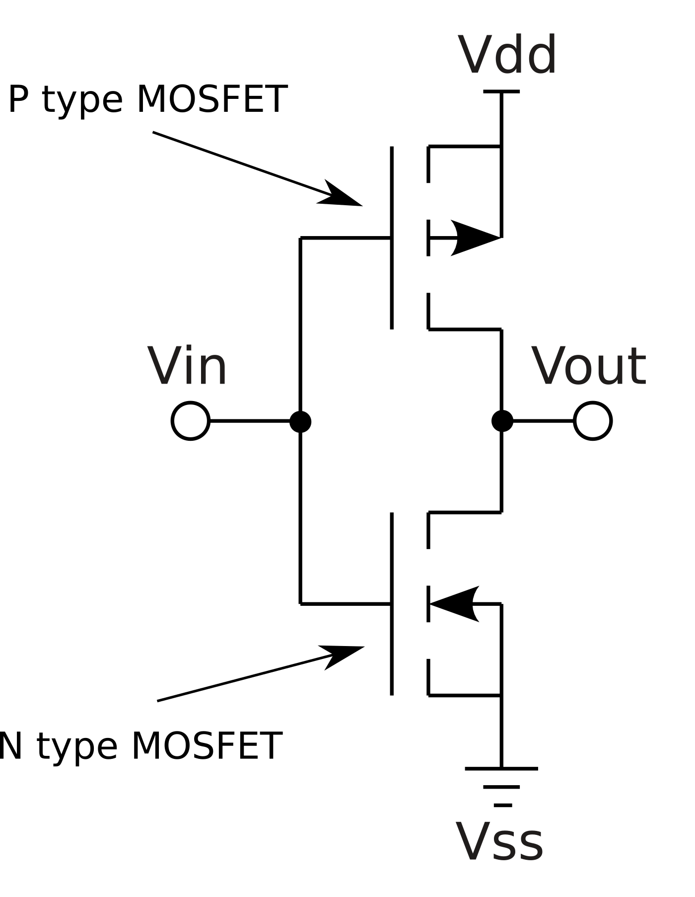
A MOSFET is a type of transistor we can use as a digital switch. The name stands for Metal Oxide Semiconductor Field Effect Transistor. The first MOSFET was made in 1959 by Mohamed M. Atalla & Dawon Kahng. The MOS part describes the gate structure, so the layering is ‘metal’ on top of an thin oxide layer, which lies on top of the (silicon) semiconductor channel. In practice the gate is typically polysilicon and not metal.| Terminology on Zero to ASIC Course
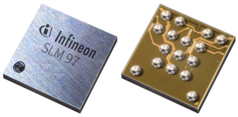
From http://88physicaldesign.blogspot.com/2015/10/what-is-macro.html: Macros are intellectual properties that you can use in your design. You do not need to design it. For example, memories, processor core, serdes, PLL etc. Macros might have a fixed function, or being parameterised. Your own design could become a fixed-function macro that some other designer could use, but a parameterised macro includes design elements and code that says how to build a macro to suit a particular set of parame...| Terminology on Zero to ASIC Course
Harden is the fancy industry word that means to take your HDL and using a tool like OpenLane turn it into the GDS2 files necessary for manufacture by a foundry.| Zero to ASIC Course
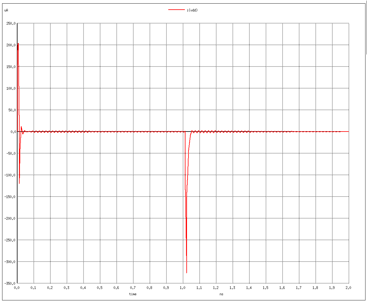
PEX stands for Parasitic Extraction (often called just ’extraction’). When we build a circuit on a chip we have an intention in mind, for example an ideal inverter inverts the incoming signal immediately and with no delay. In reality the inverter will have capacitance on both the input (due to the gate) and the output (due to the diode in the drain) and the wiring of the circuit will have both (parallel) capacitance and (series) resistance.| Zero to ASIC Course
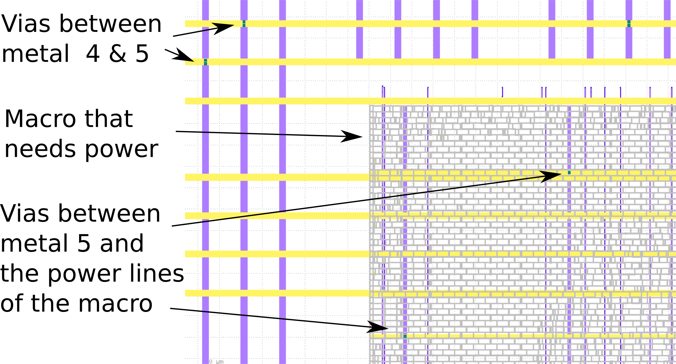
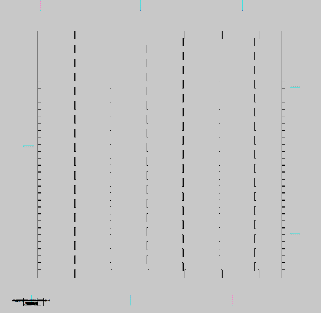
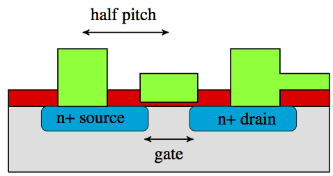
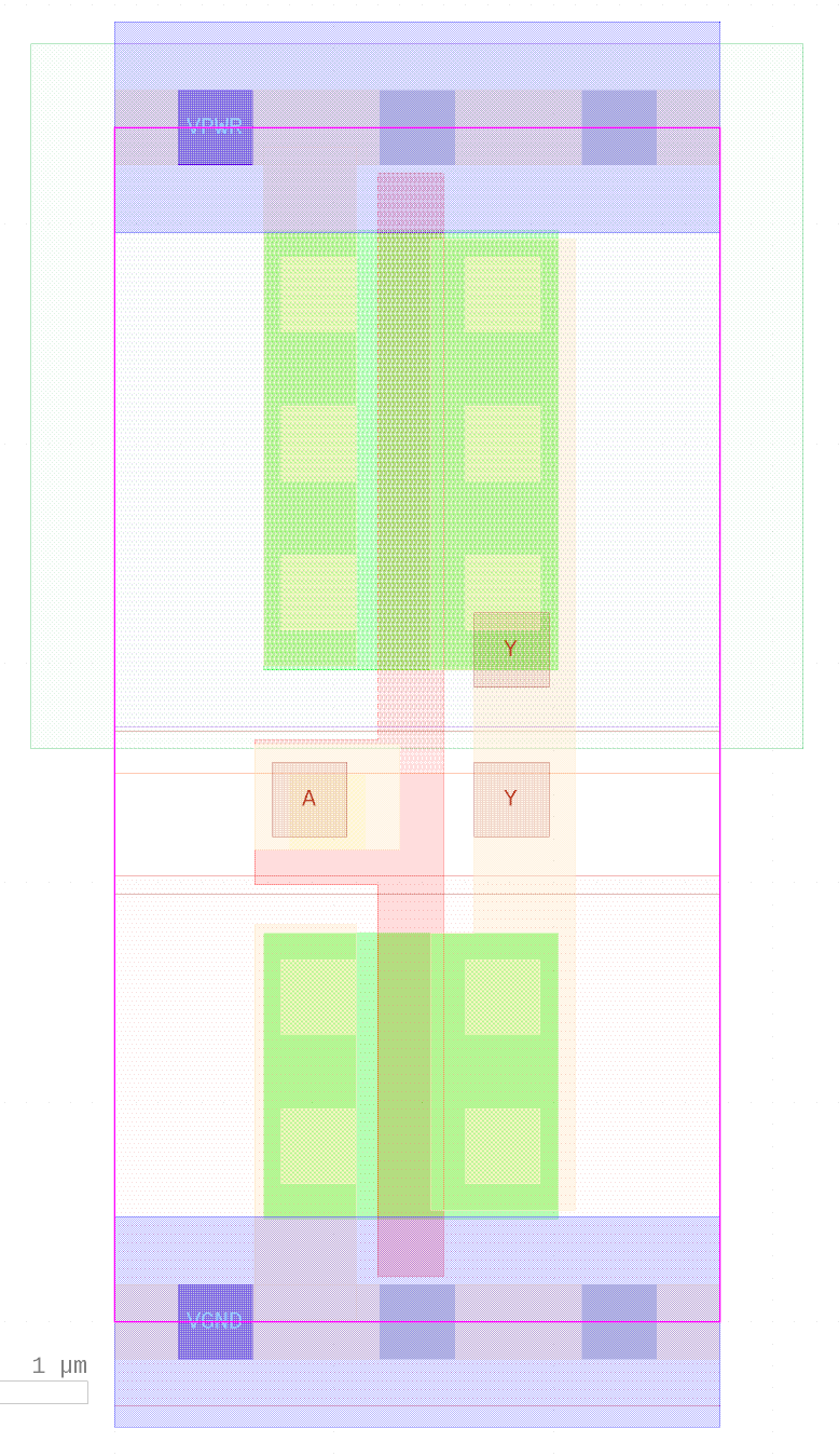
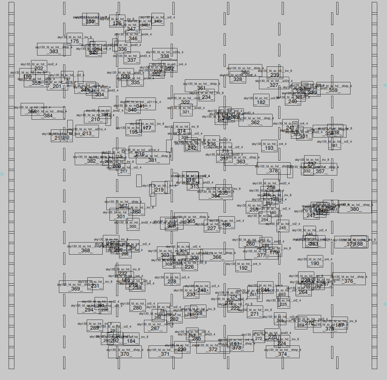
The floorplanning stage is where OpenLane decides how big an area we need to fit everything in. All the required standard cells are placed in the bottom left corner, ready for the place and route stage. All the little rectangles in the centre are called tap cells. They make sure the MOSFETs work correctly by connecting the P doped substrate to ground and the N-wells (that insulate the P-type MOSFETS) to power.| Zero to ASIC Course
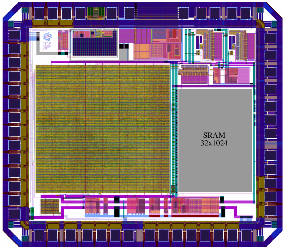
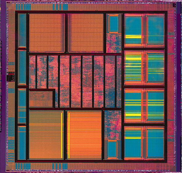
We need to make sure we can package the IC after the wafer has been diced into individual dies. A common way of packaging ICs is to connect them to a leadframe by bonding tiny wires between the leads of the leadframe and the pads on the die. The big bond pads around the outside of the IC often include ESD protection diodes, Input/Output drivers and so on. This picture shows raven, an IC from Efabless.| Zero to ASIC Course
Foundry is the fancy semiconductor word for factory. You have to admit, silicon foundry does sound cool. Another term used for this is a ‘fabrication plant’ or ‘fab’. All chips come from fabs, but when a fab is used to produce ASICs for other companies (ie the company that owns the fab is not the one that designed the chip) then it is typically referred to as a foundry. SkyWater, TSMC, Global Foundries are foundries that produce chips for many different ASIC design houses.| Zero to ASIC Course
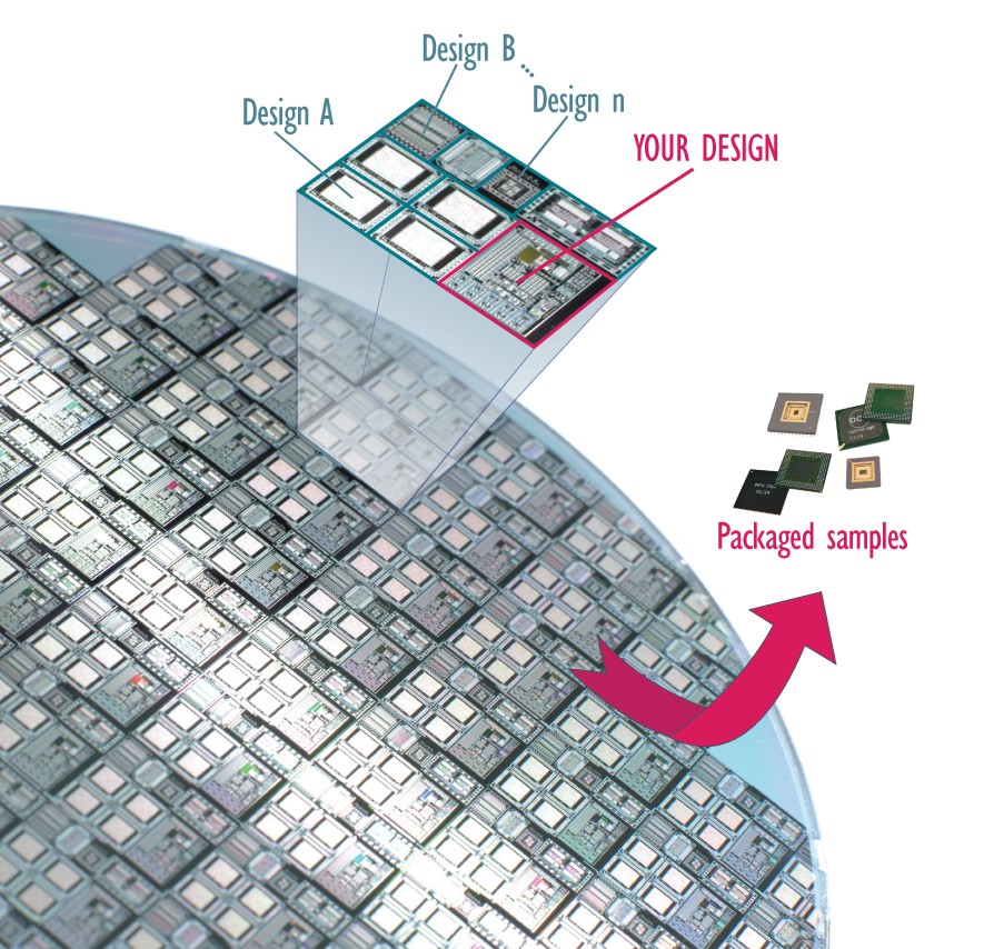
A Multi Project Wafer is used to reduce the cost of making an ASIC. By using a lot of different designs on the same wafer the Non Recurring Engineering (NRE) costs of making the mask set are shared between all the participants. The Google shuttle is an example of an MPW. Our MPW submissions So far we have made 4 tapeouts to the Google MPWs: MPW1 MPW2 MPW3 MPW4 MPW physical implementation We sent John McMaster some chips to take a look at from MPW1.| Zero to ASIC Course
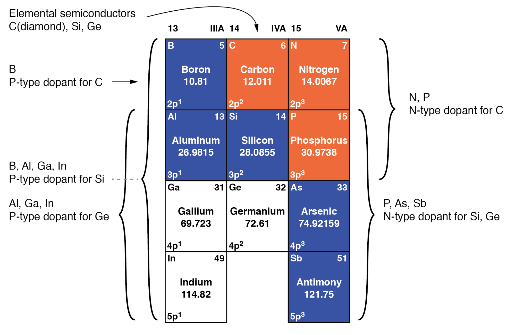
Doping is when we add impurities to the extremely pure silicon. This changes the electrochemical properties of the silicon. Silicon is in group 4 of the periodic table. Like Carbon it makes nice solid bonds in 4 directions. By adding elements from the 3rd or 5th columns we can add extra electrons or extra positive charges (holes where there are no electrons). Image source The elements we typically use are Boron for p-type (positive holes) doping and Phosphorus or Arsenic for n-type (extra ele...| Zero to ASIC Course
Silicon is purified to around 99.9999999%! Then it is sliced into very thin round sheets called wafers. The type used in the Skywater 130nm process is doped to become p-type. Here’s a great video about how silicon wafers are made. And these great videos are about the birth of the Japanese semiconductor industry. Jump to about 12 minutes in to see how they pull the silicon ingot out of the molten material.| Zero to ASIC Course
The silicon wafer is usually patterned with the mask set to make hundreds or thousands of the same IC. The circle below represents the wafer, the squares represent the copies of the maskset pattern exposed onto the wafer by the stepper. The light squares are completely within the wafer and thus may be functional chips, the others are only partial and so cannot be functional chips. Each of these ICs are then cut out of the wafer using a diamond edged saw and are called dies (or die, or dice).| Zero to ASIC Course
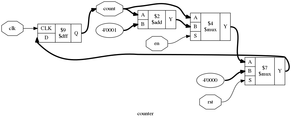
A netlist is a machine readable file that contains all the connections between all the components in your design. They are one of the outputs of a Synthesis tool like Yosys. These examples are taken from http://bygone.clairexen.net/yosys/screenshots.html If you have a counter design written in an HDL like Verilog module counter (clk, rst, en, count); input clk, rst, en; output reg [3:0] count; always @(posedge clk) if (rst) count <= 4'd0; else if (en) count <= count + 4'd1; endmodule The outp...| Zero to ASIC Course
An Integrated Circuit is a collection of circuit elements all together on one piece of silicon. Example elements include: transistors, for example MOSFETS resistors capacitors inductors Here is an example of a fairly small IC, a type of amplifier called an Op-Amp. The image is from zeptobars The orange zig-zag elements are resistors, the large areas at the top are capacitors, the squares with circular elements in their centres are bipolar transistors, and the thin silver elements are wires jo...| Zero to ASIC Course
Synthesis converts a behavioral description of the circuit, in the form of RTL, into an equivalent netlist made of cells from the standard cell library. It is analogous to the compilation process used for turning programming languages like C into binaries. The compiler knows how to read the language and maps it to the instructions we have available in the CPU, and synthesis translates from what we want the design to do, into a set of available cells that will perform it.| Zero to ASIC Course
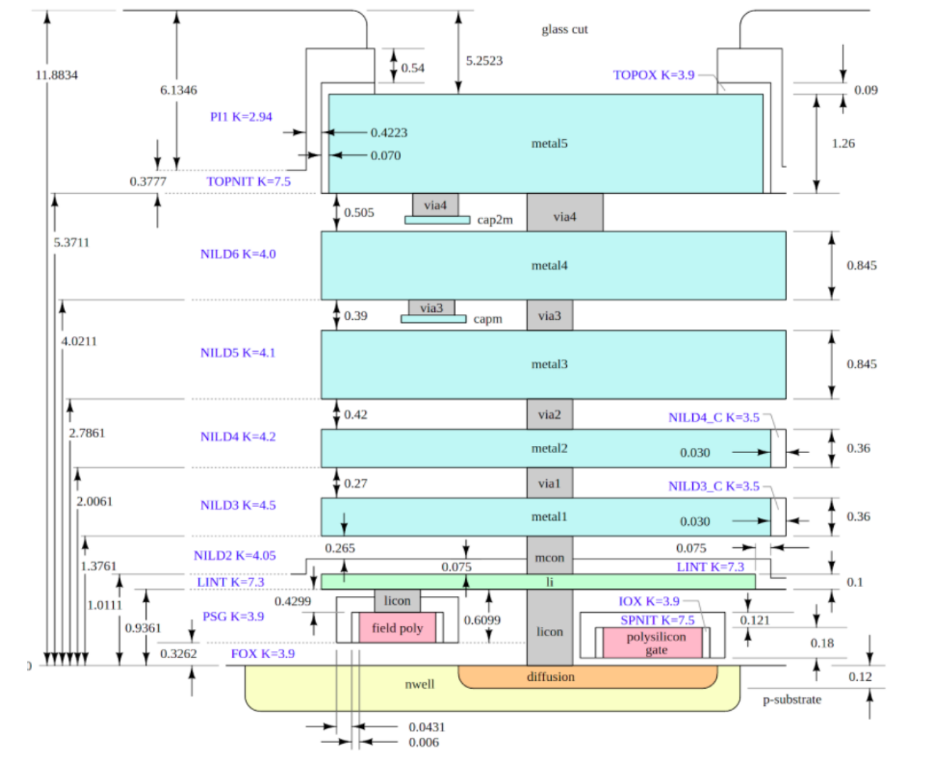
The Design Rule Check is part of the PDK. Both the Magic and OpenLane tools make use of it. It contains rules that check things like: The gate of the MOSFET are the correct dimensions, Wires on the metal layers are not too narrow and not too close, Check that MOSFET gates are protected if they have long connecting wires - this is called an antenna rule. The design rules are generally a description of the smallest items that can be reliably manufactured so that a whole chip is functional.| Zero to ASIC Course
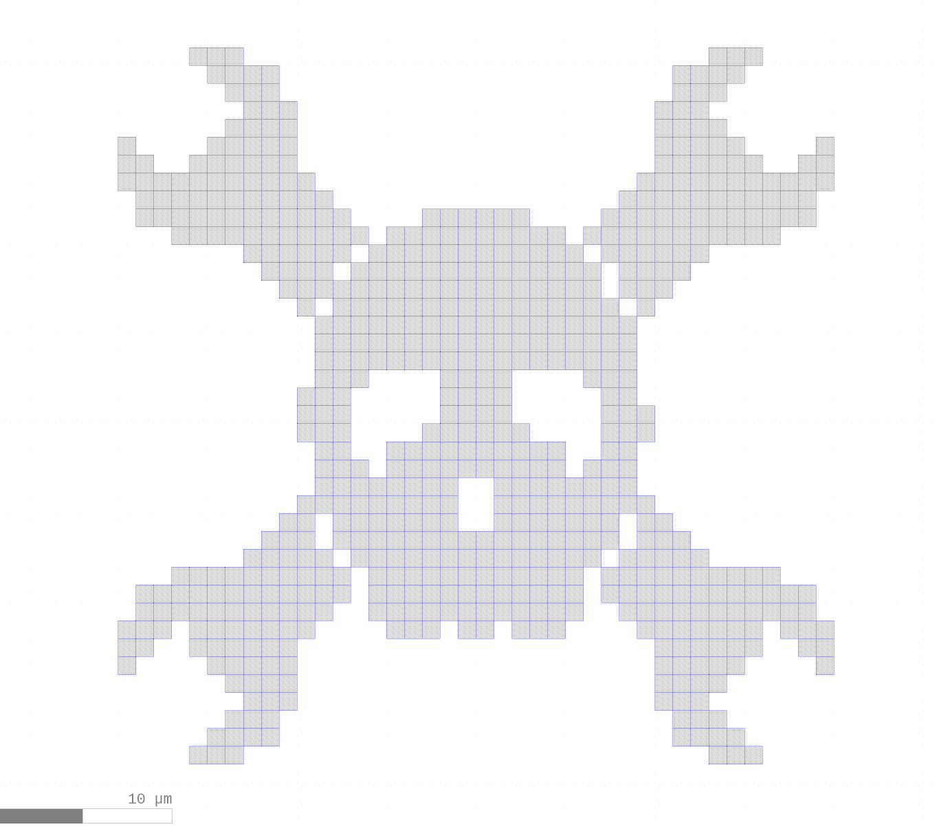
GDSII/GDS2 is a binary file format that represents the layers needed to produce an ASIC. In the OpenLane flow, Magic is used to ‘stream’ the final GDS2 files. All shapes are assigned to a given GDS2 layer, and each layer ends up being used to create a mask, although often this may involve the combination of one or more GDS2 layers to form one mask, and the shapes are often grown, or shrunk, or merged and thus what ends up on the mask may not be the same as what was drawn by the designer.| Zero to ASIC Course
Once a chip design is complete, it is taped out for manufacturing. This means sending the GDS2 files to the foundry. The term “tape out” was coined in 70’s. There are 2 theories from where the name comes from: Early ICs were made in a very similar process to PCBs, where sticky tape was used to create the shapes, followed by shrinking the design down with an optical photograpy process. ASIC design files were stored on magnetic tape.| Zero to ASIC Course
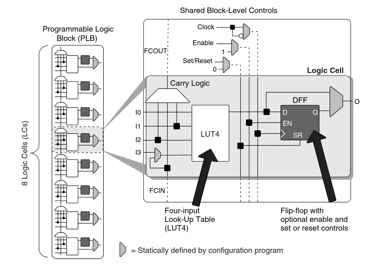
One of the many things a PDK contains is the standard cell library. This is a collection of all digital building blocks used to build an IC like AND, OR, NOT gates, flip-flops, etc. There will be other libraries for specialised functions such as IO pads, and any analogue blocks or memory macros, and so on. Standard cell libraries are a set of cells that have common characteristics and physical layout.| Zero to ASIC Course
Application Specific Integrated Circuit. An ASIC is a custom IC, which means it is not a standard product such as a microprocessor, memory, standard logic chip or generic component which might be available from several or many different manufacturers. It will often add functionality not available from a standard product, or combine the functions of many standard products at a lower total price. You might make an ASIC because: You need a chip that isn’t available off-the-shelf, You can save ...| Zero to ASIC Course
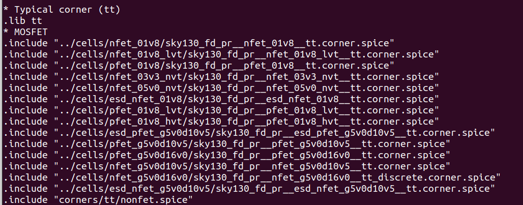
MOSFET characteristics can vary across multiple wafers. If we wanted to make sure a sensitive analogue design worked across all process variations, we would want to simulate these variations and check the results were still within our specification. Some of the most common variations affect the strength or speed of the MOSFET switching, and we have both P and N type MOSFETS. The corners represent the most extreme variations of these parameters.| Zero to ASIC Course
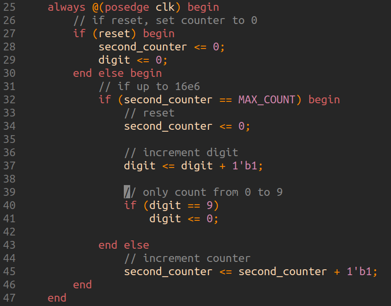
A Hardware Description Language is used to… describe hardware! So instead of drawing out an inverter using a tool like Magic we can write a line like this: output = !input; Which describes what an inverter does. The ! means invert. This is a description of what the circuit does, similar to a programming language like C (although everything happens at once, not in sequence). This is referred to as a ‘Register Transfer Level’ or RTL.| Zero to ASIC Course
Sam Zeloof did a great talk about his home IC foundry at the Hackaday Supercon 2019. This slide shows an overview of the process: A series of masks is used to build up a 3 dimensional structure on the wafer. Each step is fundamentally the same: Deposit a layer of silicon dioxide (glass) on the surface of the wafer Coat the glass with photoresist (which is a light sensitive organic compound, similar to photographic emulsion) Bake it Use a mask to cover certain areas and use light (often UV) to...| Zero to ASIC Course
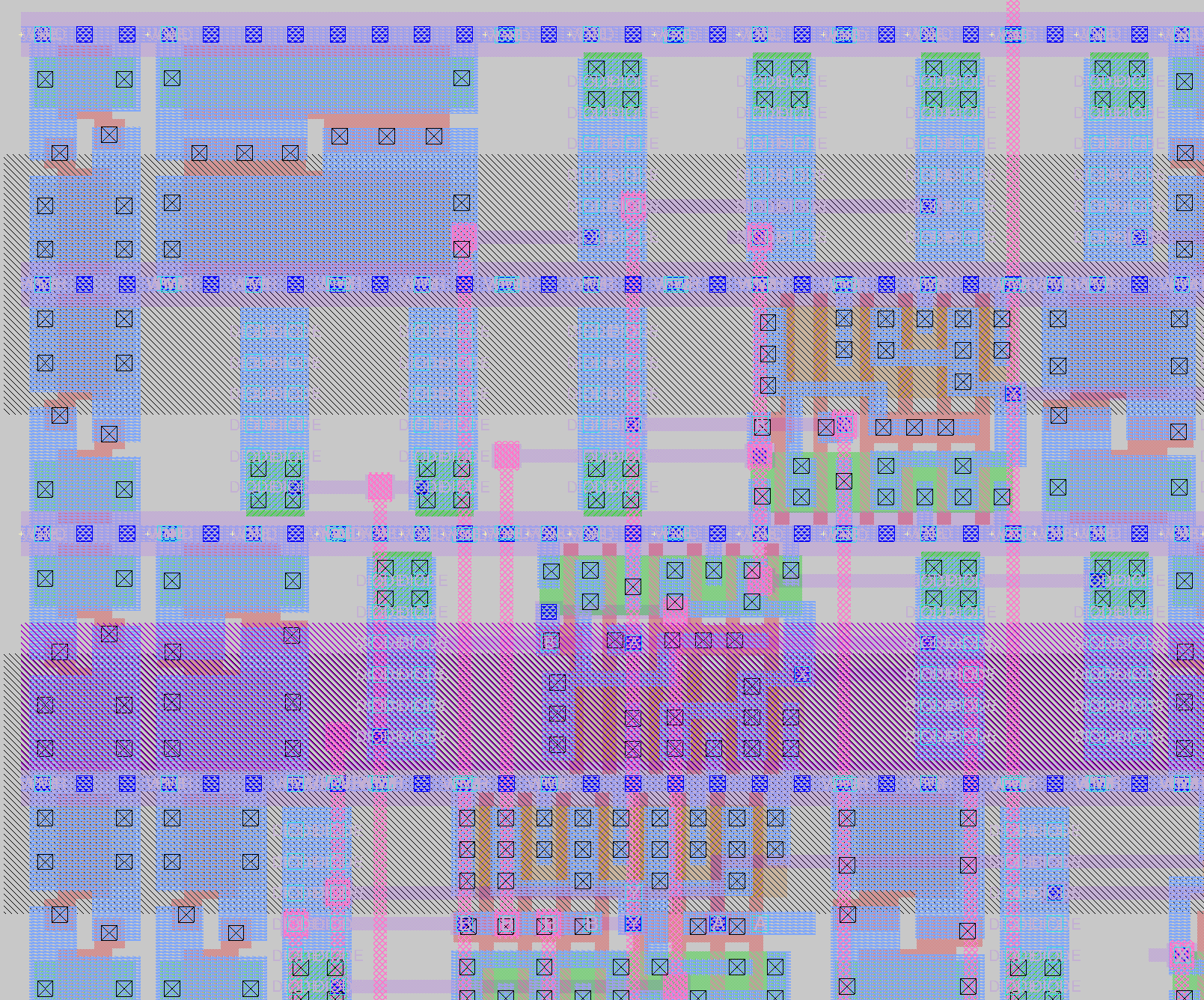
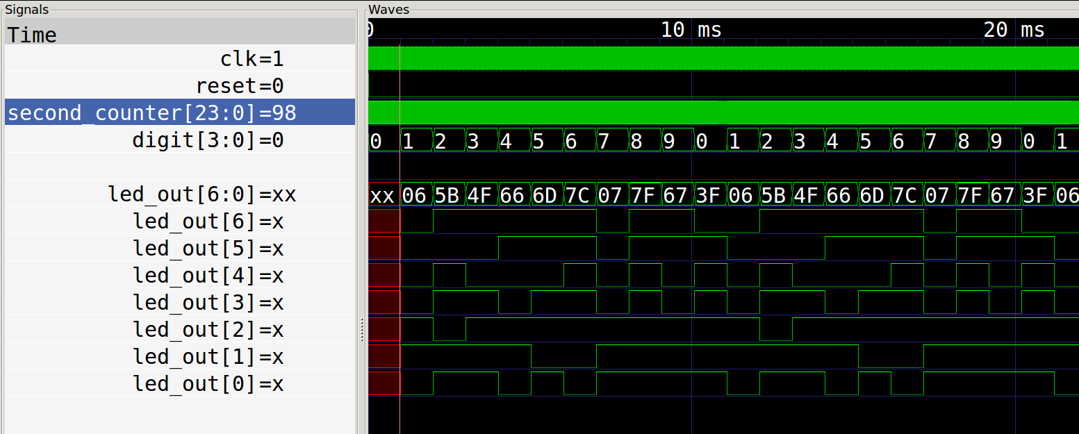
Place and Route are two steps in the automated process of turning some HDL into GDS2 files. We will look at how OpenLane does these steps using the seven segment seconds example. I have used my presentation tools to generate these images. Place Placement is done in two steps, coarse and fine. The coarse step puts the standard cells in roughly the right place. This may be referred to as global placement, or initial placment. The aim here is to minimise the estimated total wire length of all th...| Zero to ASIC Course
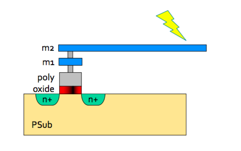
Antenna rules are part of the DRC. When the ASIC is being built up layer by layer, we have the gates of the MOSFETS built first. Then we use the metal layers to connect them into bigger blocks. The metal layers are etched using a plasma which is made of ionised atoms, and the electrical charge from this can build up on already existing wires. The more static charge that builds up, the higher the voltage that is seen.| Zero to ASIC Course